Patents
Literature
Hiro is an intelligent assistant for R&D personnel, combined with Patent DNA, to facilitate innovative research.
4415 results about "Quantum efficiency" patented technology
Efficacy Topic
Property
Owner
Technical Advancement
Application Domain
Technology Topic
Technology Field Word
Patent Country/Region
Patent Type
Patent Status
Application Year
Inventor
The term quantum efficiency (QE) may apply to incident photon to converted electron (IPCE) ratio, of a photosensitive device or it may refer to the TMR effect of a Magnetic Tunnel Junction. This article deals with the term as a measurement of a device's electrical sensitivity to light. In a charge-coupled device (CCD) it is the percentage of photons hitting the device's photoreactive surface that produce charge carriers. It is measured in electrons per photon or amps per watt. Since the energy of a photon is inversely proportional to its wavelength, QE is often measured over a range of different wavelengths to characterize a device's efficiency at each photon energy level. The QE for photons with energy below the band gap is zero. Photographic film typically has a QE of much less than 10%, while CCDs can have a QE of well over 90% at some wavelengths.
Light emitting material and organic light-emitting device
InactiveUS7396598B2High efficiency of light emissionKeep energy smallDischarge tube luminescnet screensGroup 8/9/10/18 element organic compoundsFluorescenceTriplet state
Owner:SAMSUNG ELECTRONICS CO LTD
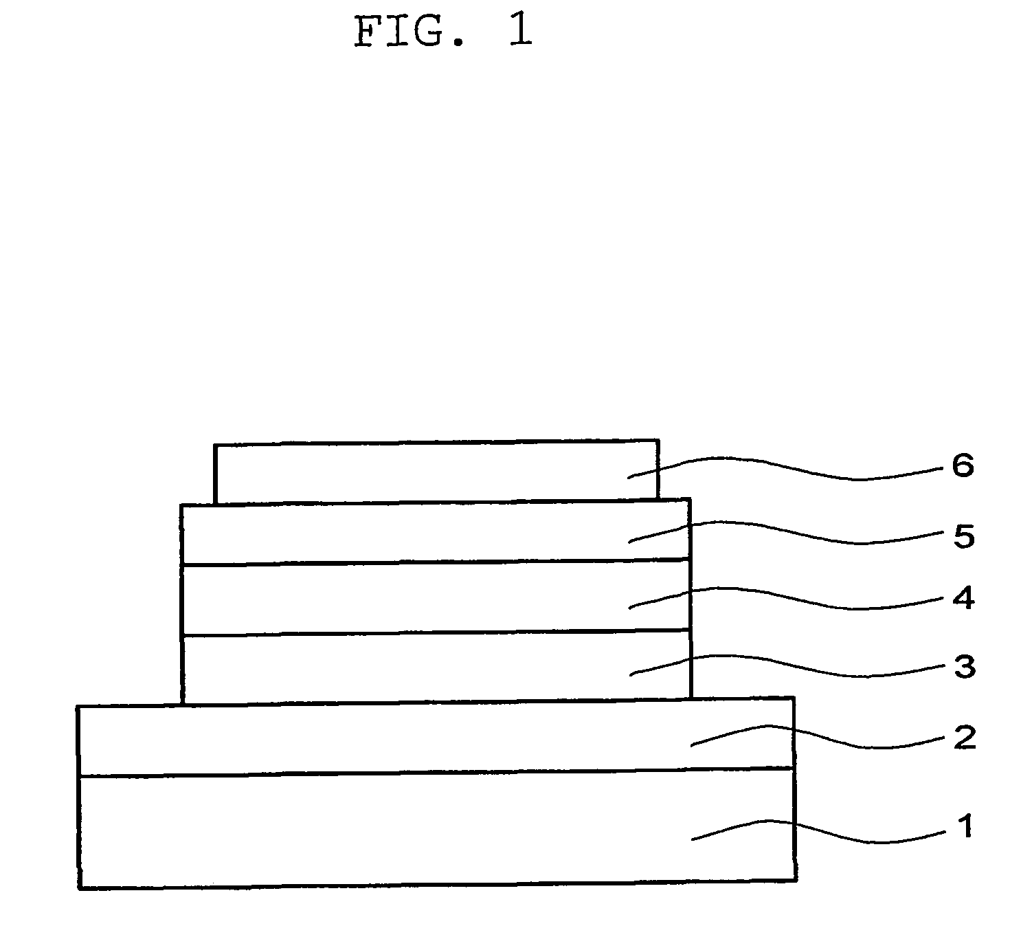
Red phosphorescent compounds and organic electroluminescent devices using the same
ActiveUS20090104472A1Good red color puritySolve low luminous efficiencyIndium organic compoundsElectroluminescent light sourcesQuantum efficiencyOrganic electroluminescence
Provided are red phosphorescent compounds represented by Formula 1:Organic electroluminescent devices using the red phosphorescent compounds are further provided. The organic electroluminescent devices exhibit good red color purity, high quantum efficiency, high power efficiency, high luminance, and long lifetime.
Owner:SAMSUNG ELECTRONICS CO LTD
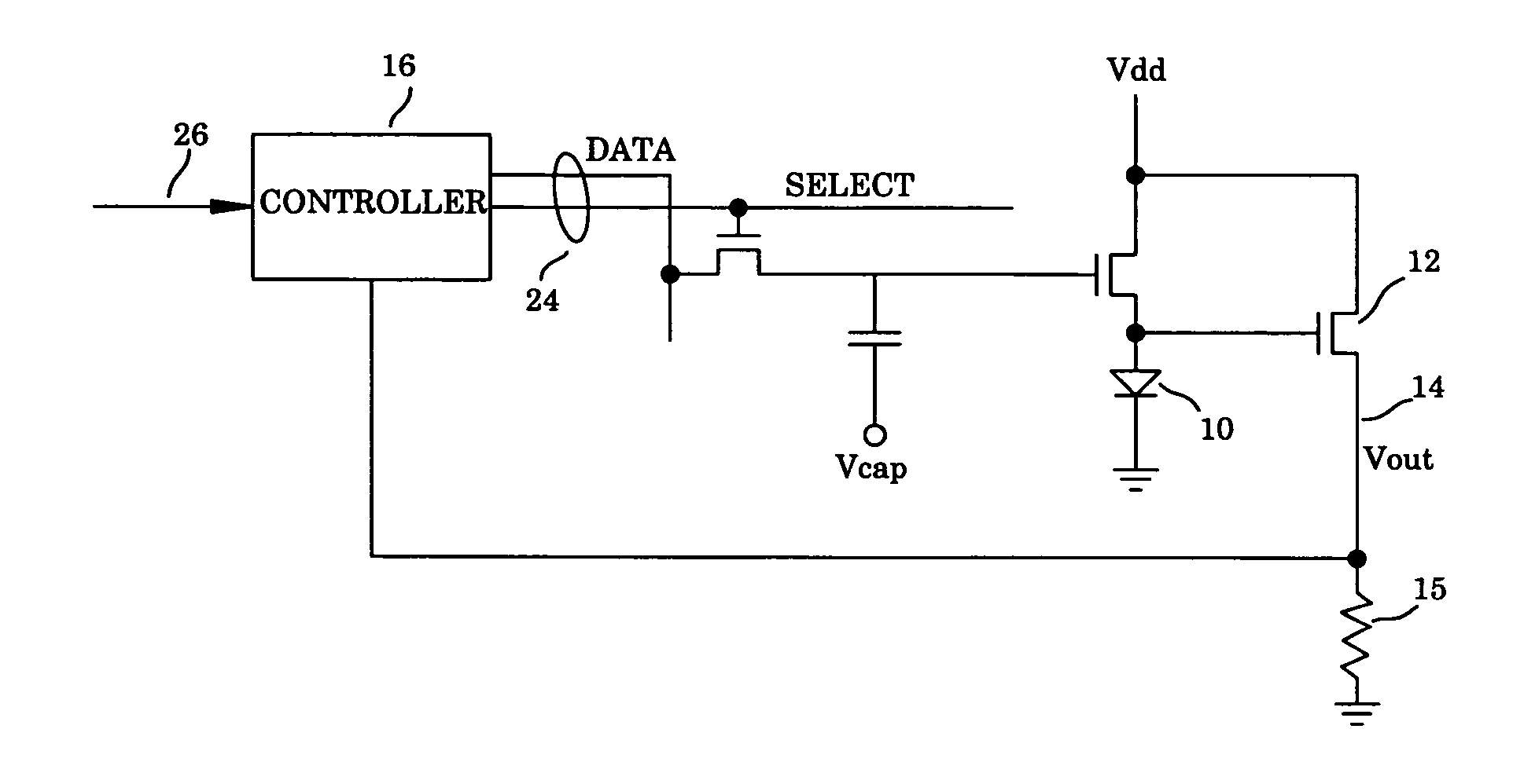
Method and apparatus for managing and uniformly maintaining pixel circuitry in a flat panel display
InactiveUS20080048951A1Accurate aging correctionStatic indicating devicesQuantum efficiencyDisplay design
The present invention describes a method and apparatus for measuring the voltage and current characteristics of the OLED pixel as it ages and correlating the measured data to the decrease in quantum efficiency and changes in OLED impedance over the life of the OLED, so that corrections can be made to the image drive system to prevent image sticking and color point drift. The method and apparatus of the present invention do not require any additional circuitry or changes in the display design. The circuitry of the present invention is implemented in the display driver integrated circuit (IC) chips. The basis of the invention is the luminance-current-voltage (LIV) curves which characterize the OLED materials over their life time. A series of these curves are stored in memory representing a OLED material at various ages. The apparatus of the present invention is used to measure driver voltages and currents for a pixel having an OLED, which measurements are then used to extract the voltage current curve for the OLED at any point in time. The extracted curve is compared to the aging curves stored in memory to determine the aging curve that best describes the measured present voltage current characteristic of the pixel. That aging curve is used to drive the pixel.
Owner:LEADIS TECH
Nanocrystal doped matrixes
ActiveUS20070034833A1Good miscibilityInhibit aggregationMaterial nanotechnologyIndividual molecule manipulationAnti-reflective coatingSemiconductor nanocrystals
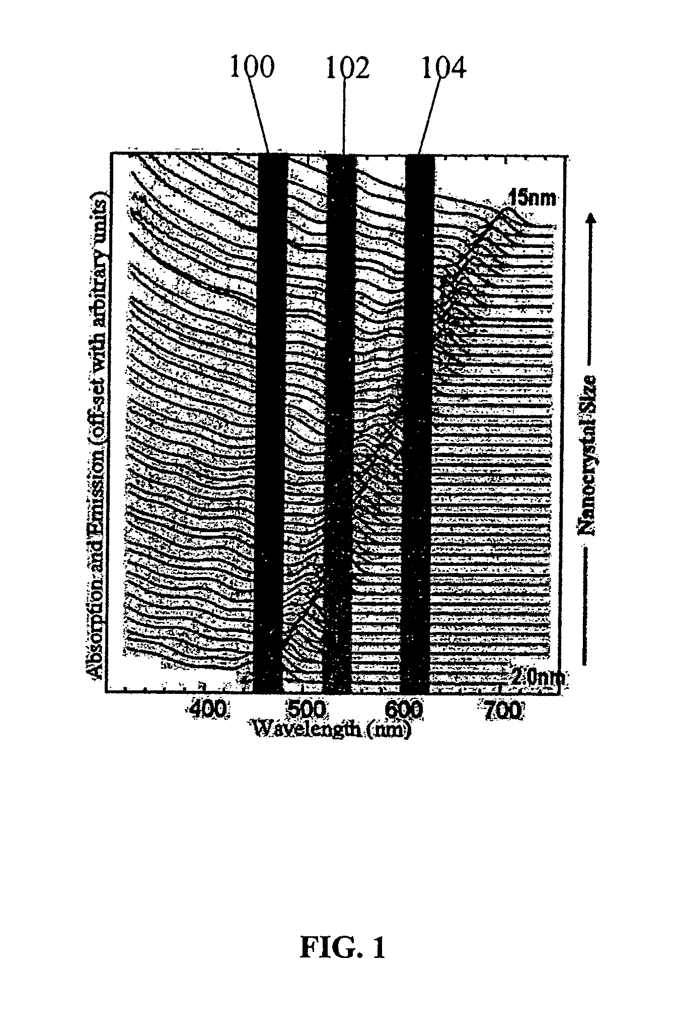
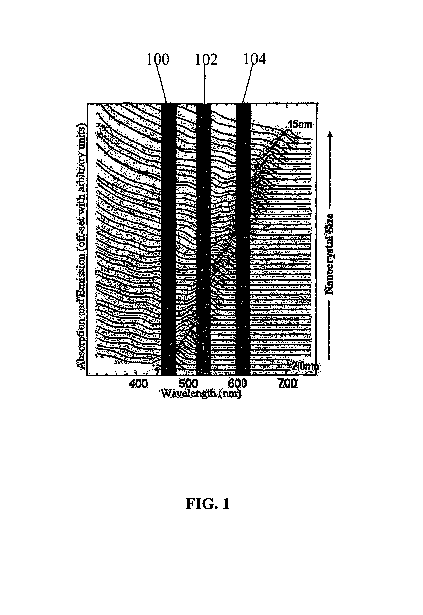
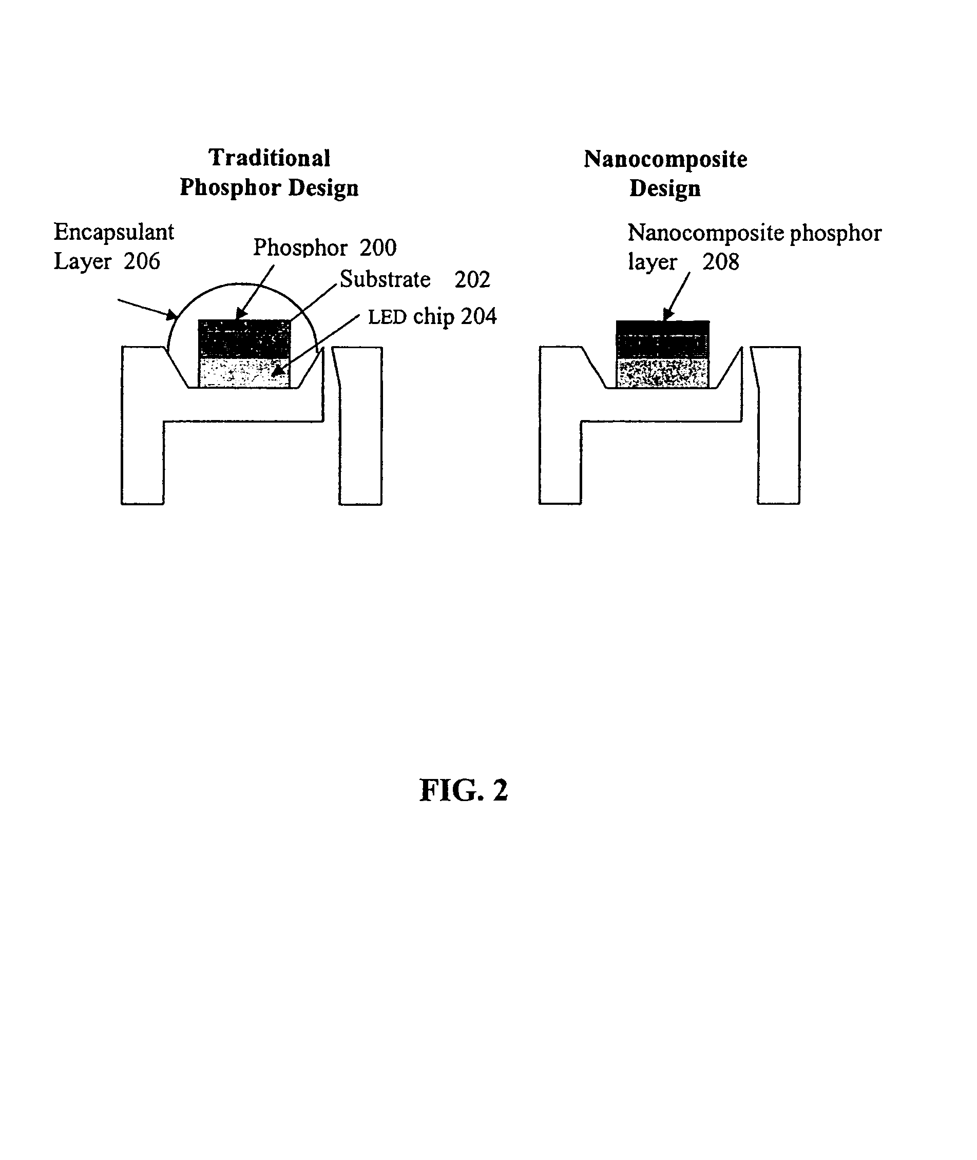
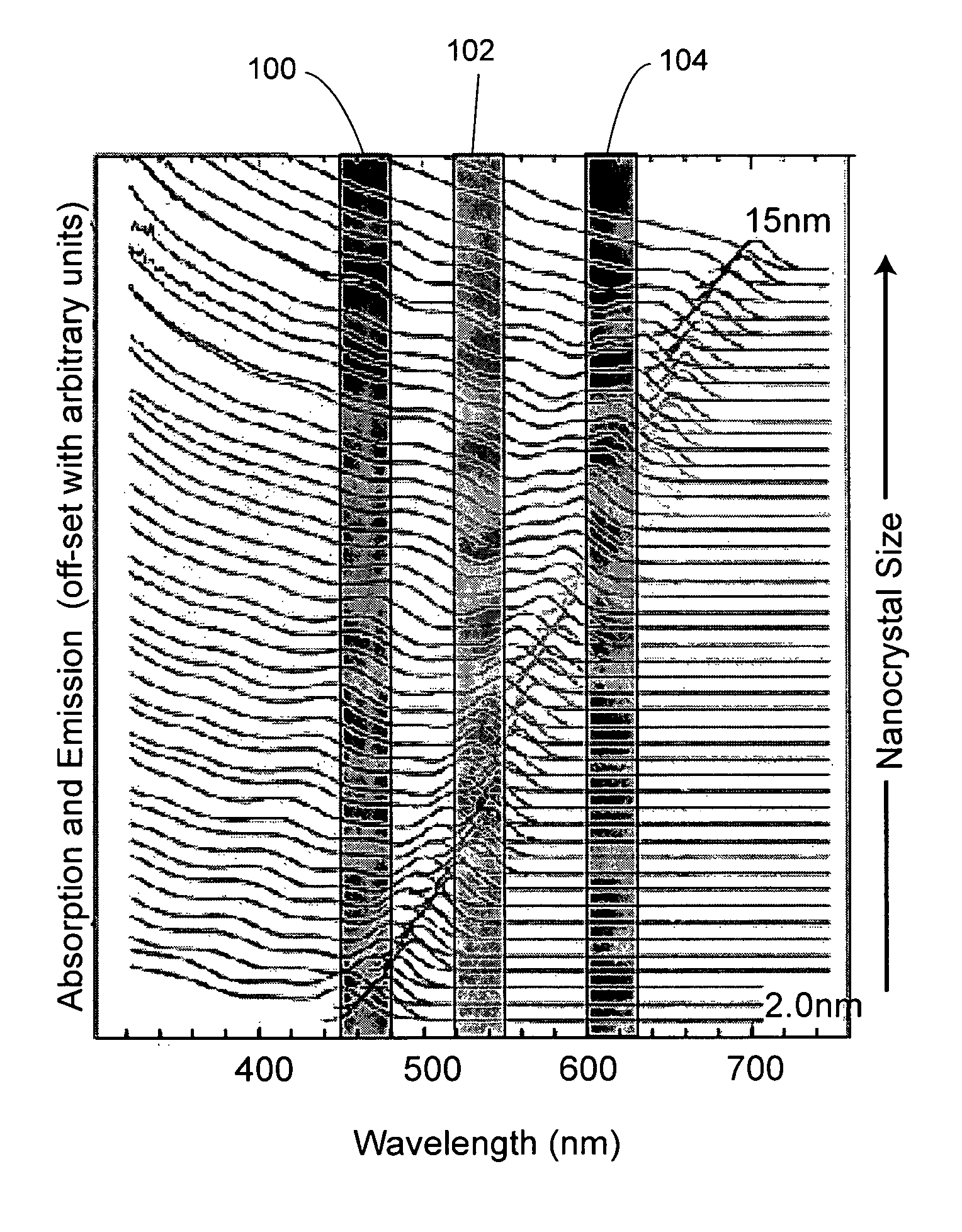
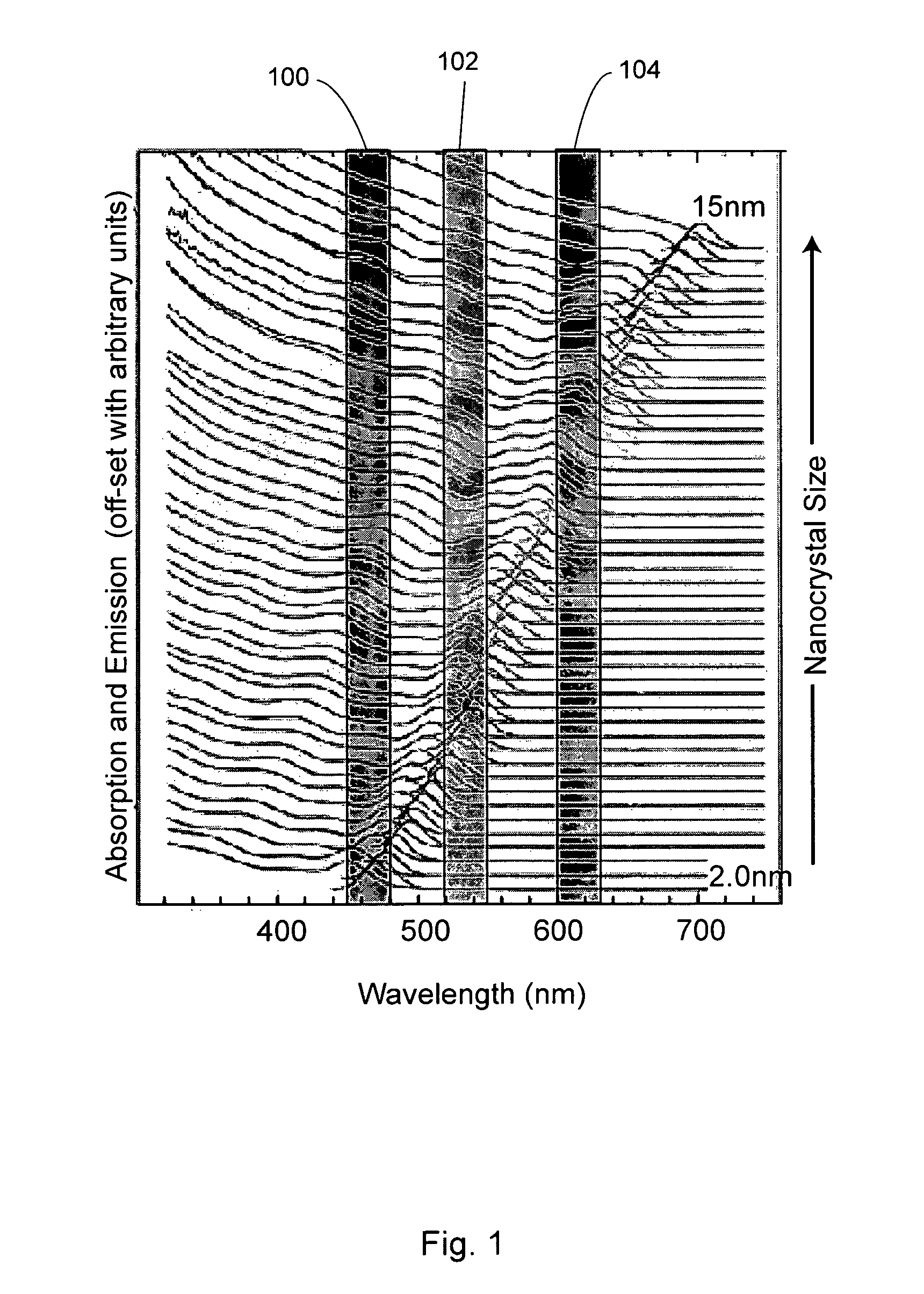
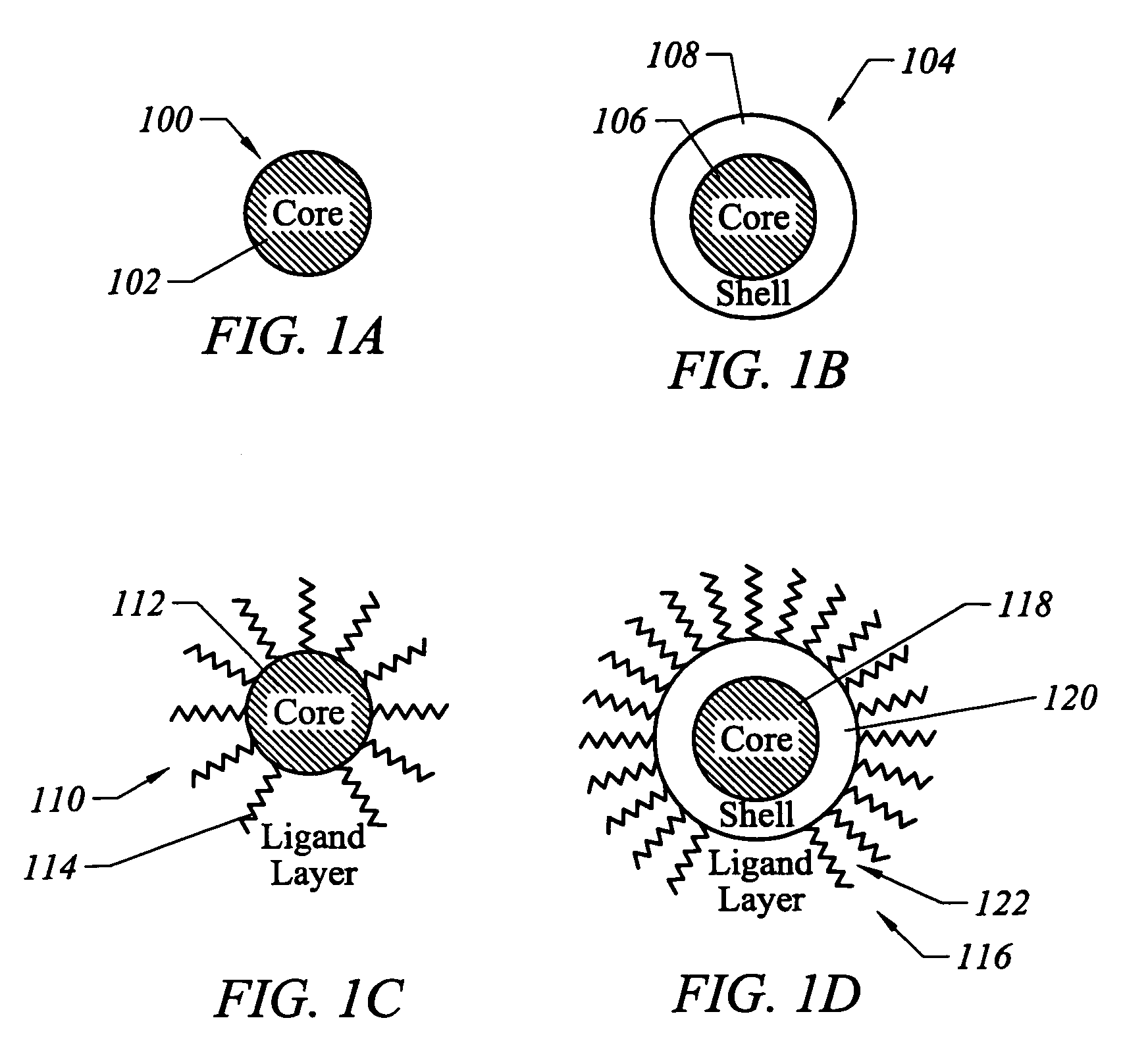
Matrixes doped with semiconductor nanocrystals are provided. In certain embodiments, the semiconductor nanocrystals have a size and composition such that they absorb or emit light at particular wavelengths. The nanocrystals can comprise ligands that allow for mixing with various matrix materials, including polymers, such that a minimal portion of light is scattered by the matrixes. The matrixes of the present invention can also be utilized in refractive index matching applications. In other embodiments, semiconductor nanocrystals are embedded within matrixes to form a nanocrystal density gradient, thereby creating an effective refractive index gradient. The matrixes of the present invention can also be used as filters and antireflective coatings on optical devices and as down-converting layers. Processes for producing matrixes comprising semiconductor nanocrystals are also provided. Nanostructures having high quantum efficiency, small size, and / or a narrow size distribution are also described, as are methods of producing indium phosphide nanostructures and core-shell nanostructures with Group II-VI shells.
Owner:SAMSUNG ELECTRONICS CO LTD
Optical devices featuring textured semiconductor layers
ActiveUS20070120141A1Accelerate escapeLight extraction efficiencySolid-state devicesNanoopticsQuantum efficiencyPhosphor
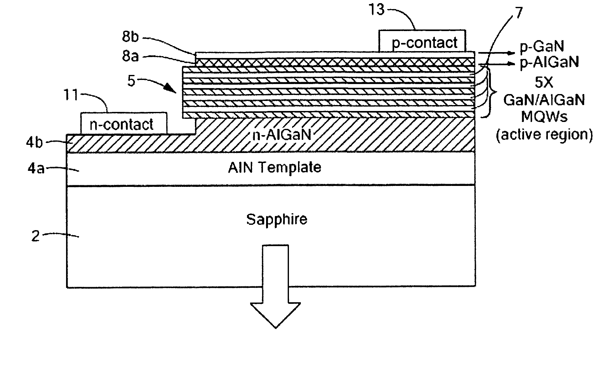
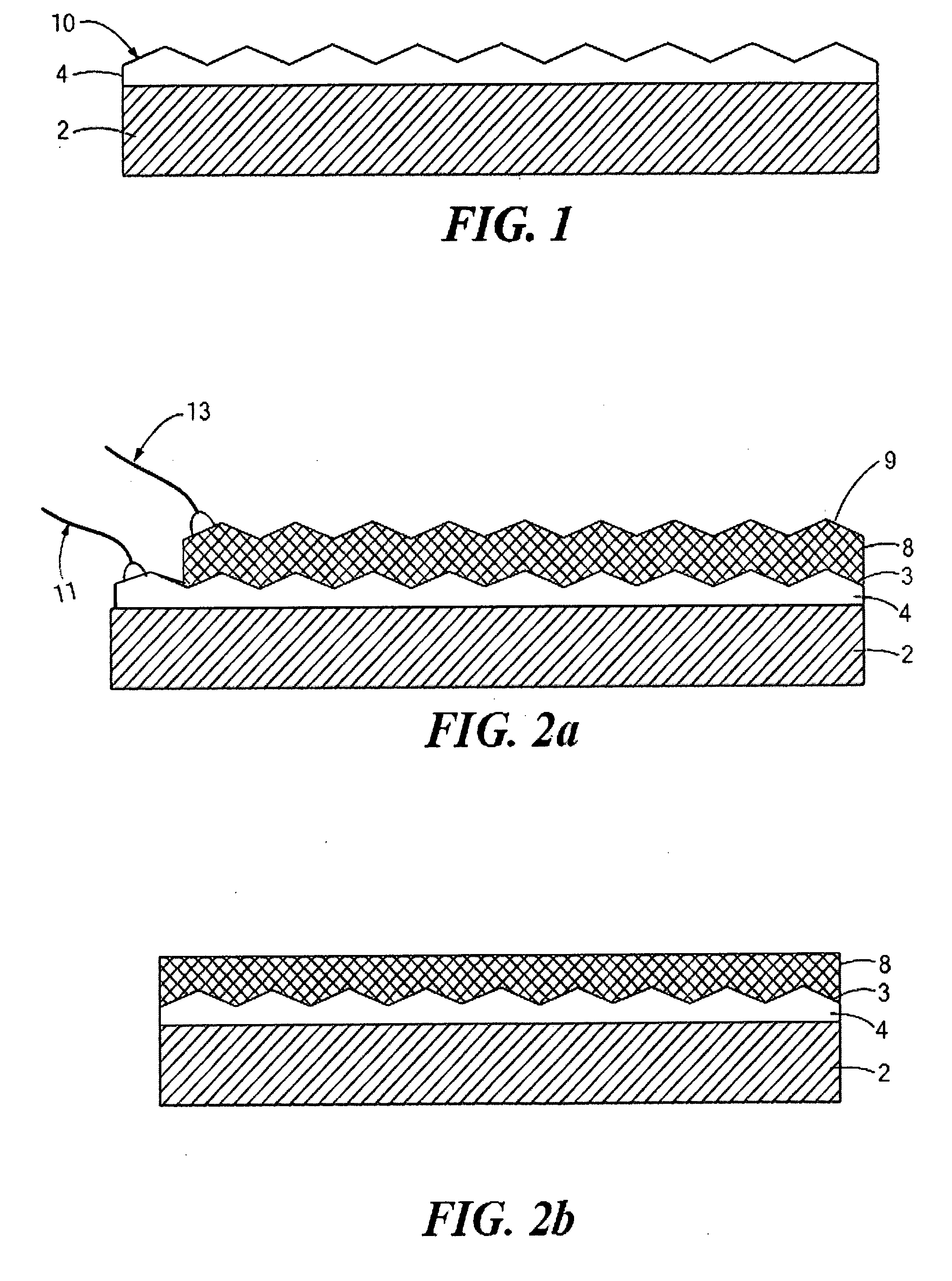
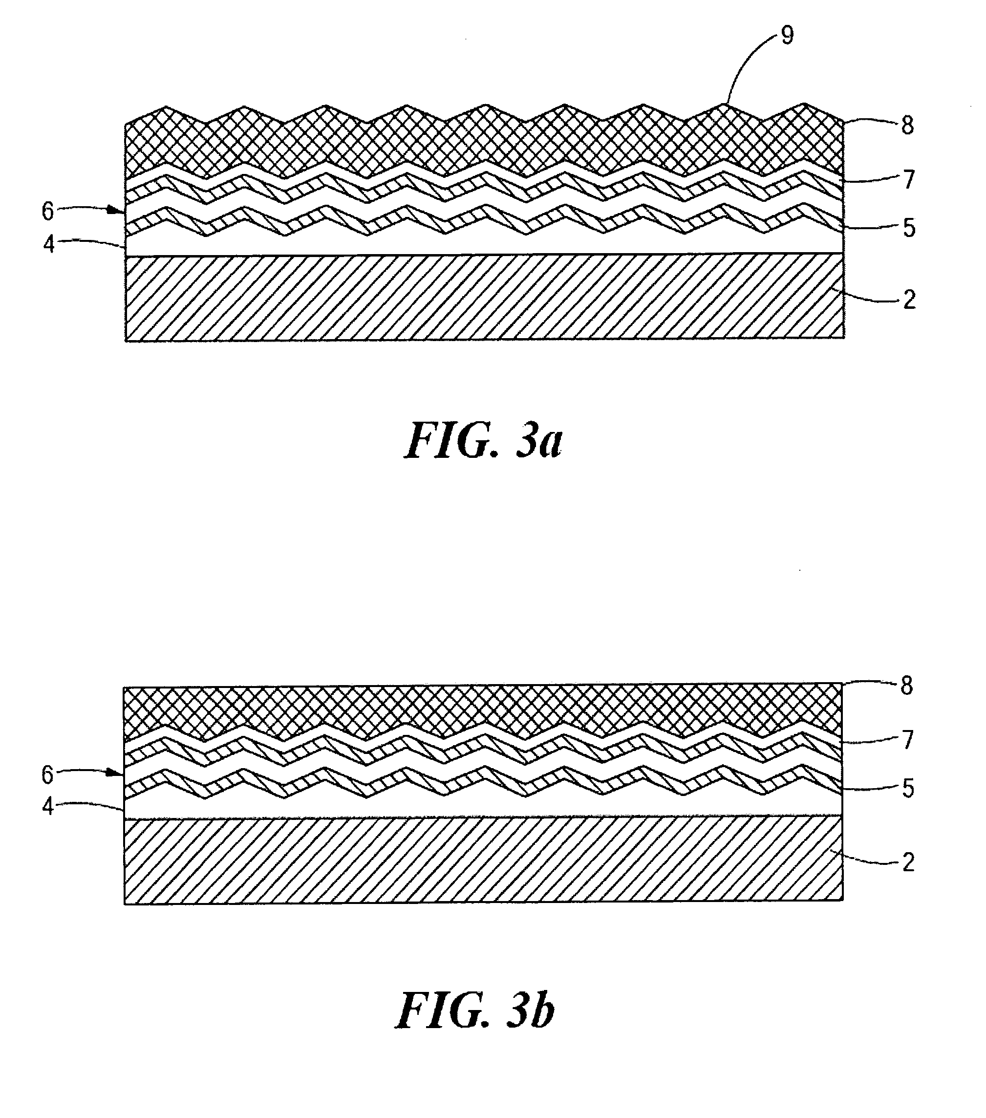
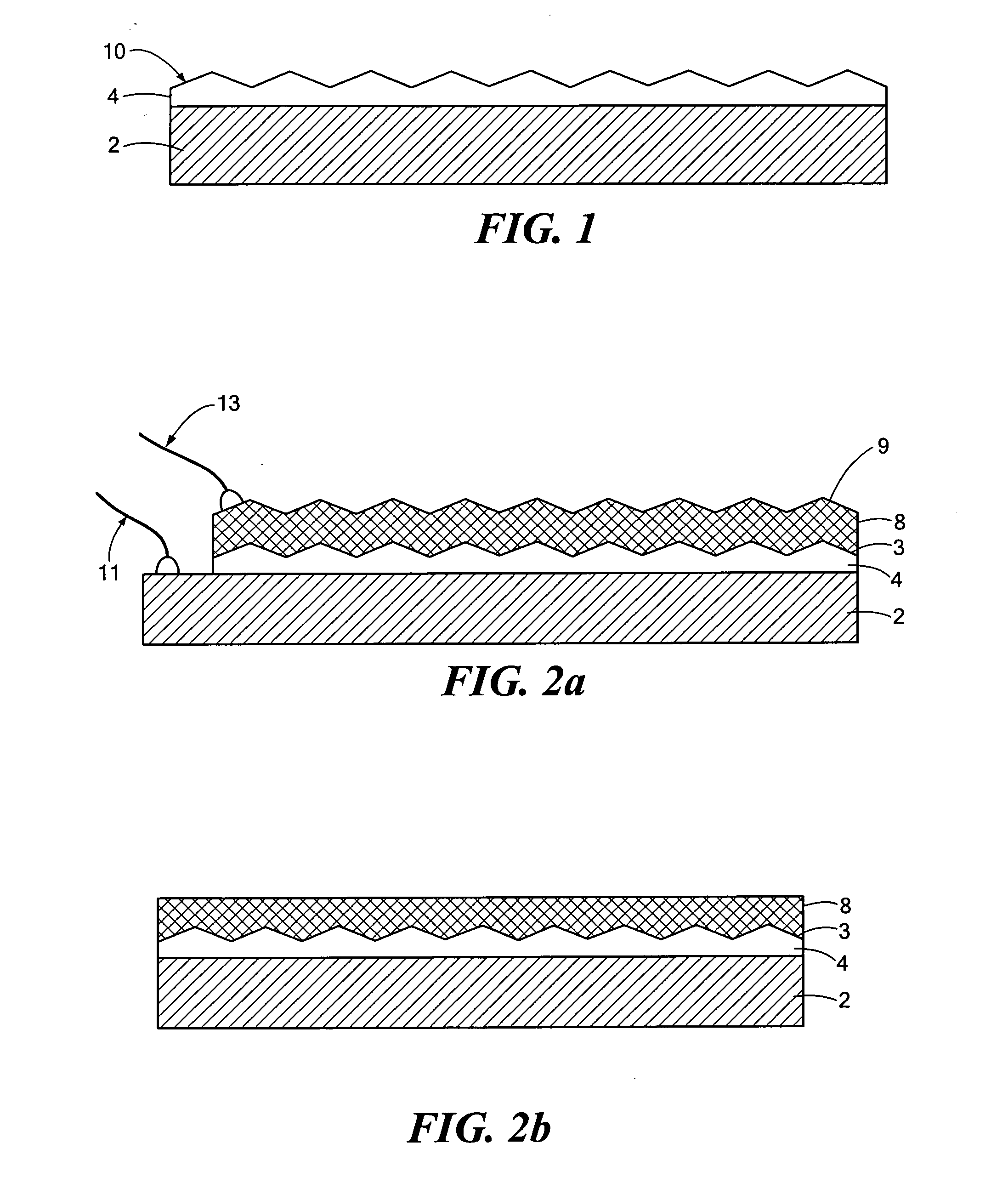
A semiconductor sensor, solar cell or emitter, or a precursor therefor, has a substrate and one or more textured semiconductor layers deposited onto the substrate. The textured layers enhance light extraction or absorption. Texturing in the region of multiple quantum wells greatly enhances internal quantum efficiency if the semiconductor is polar and the quantum wells are grown along the polar direction. Electroluminescence of LEDs of the invention is dichromatic, and results in variable color LEDs, including white LEDs, without the use of phosphor.
Owner:TRUSTEES OF BOSTON UNIV
Nanocrystal doped matrixes
ActiveUS7645397B2Good miscibilityInhibit aggregationMaterial nanotechnologyIndividual molecule manipulationAnti-reflective coatingQuantum efficiency
Owner:SAMSUNG ELECTRONICS CO LTD
Semiconductor light emitting device
InactiveUS20030057444A1Blocking may occurAvoid defectsSemiconductor/solid-state device detailsSolid-state devicesQuantum efficiencyCrystallographic defect
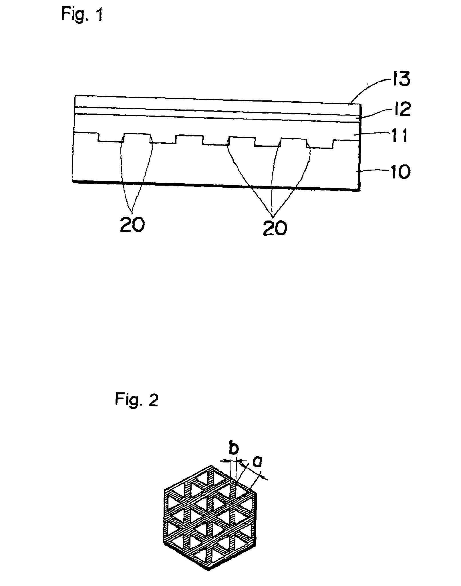
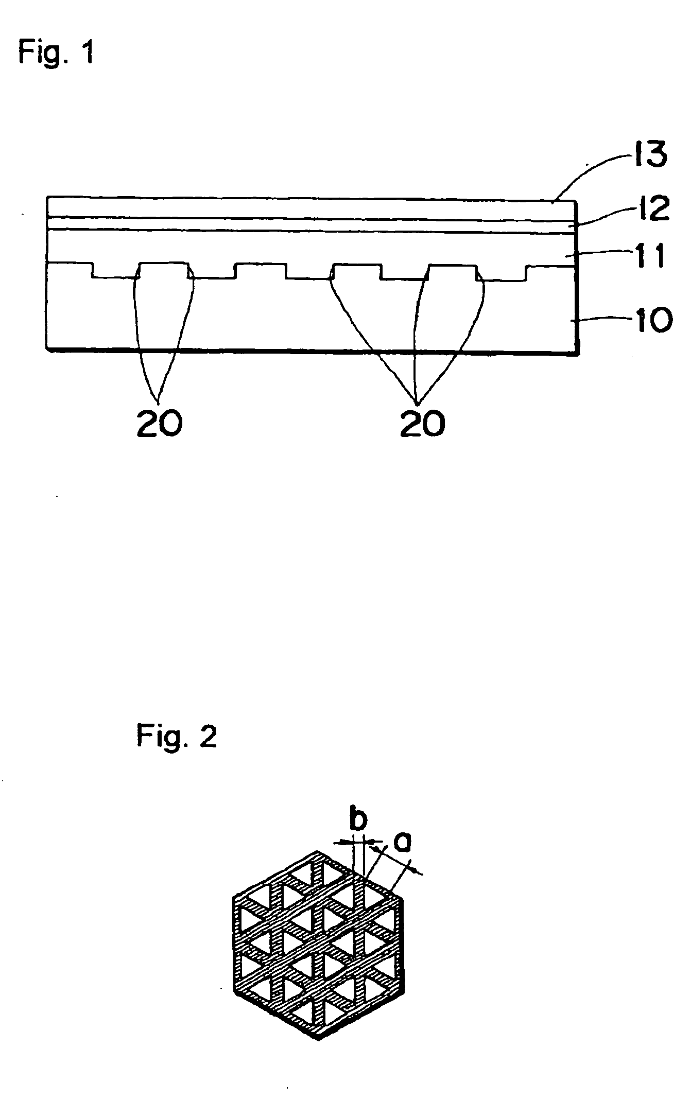
A high external quantum efficiency is stably secured in a semiconductor light emitting device. At least one recess and / or protruding portion is created on the surface portion of a substrate for scattering or diffracting light generated in a light emitting region. The recess and / or protruding portion has a shape that prevents crystal defects from occurring in semiconductor layers.
Owner:NICHIA CORP
Functionalized matrixes for dispersion of nanostructures
ActiveUS20100276638A1High quantum yieldFacilitate device fabricationMaterial nanotechnologyGroup 4/14 element organic compoundsAnti-reflective coatingVolumetric Mass Density
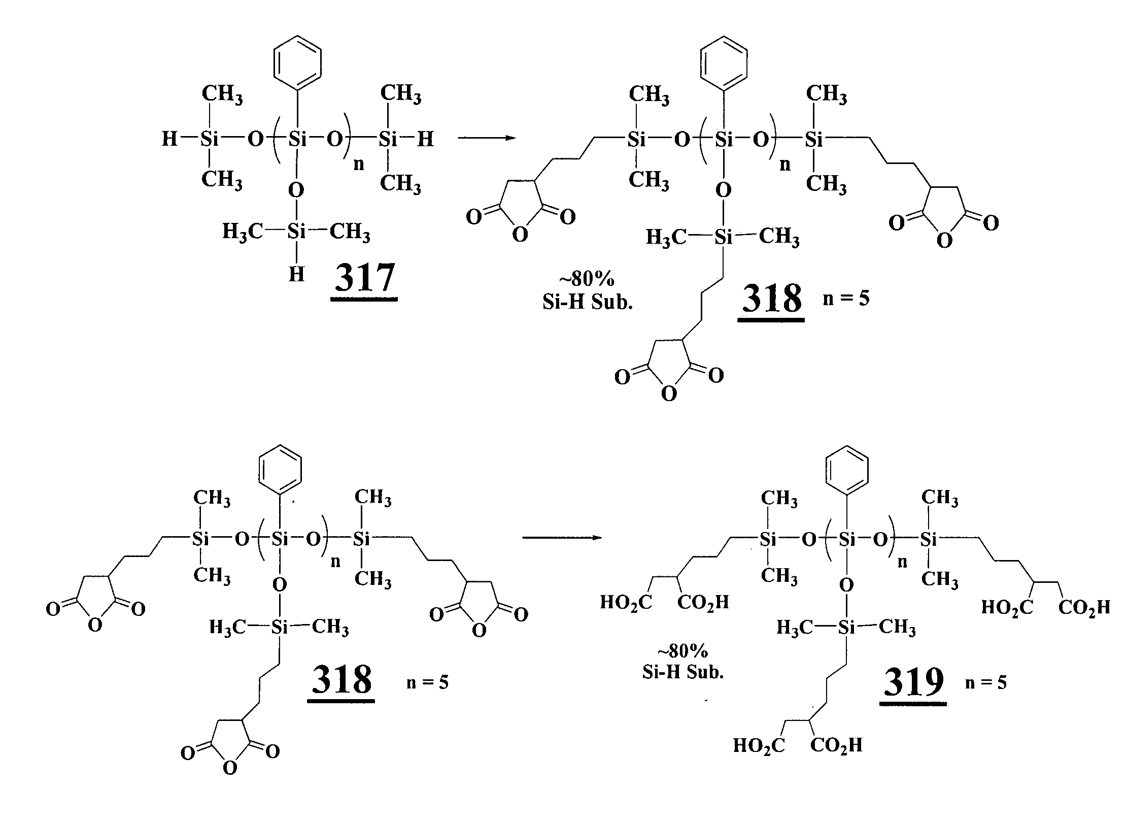
Matrixes doped with semiconductor nanocrystals are provided. In certain embodiments, the semiconductor nanocrystals have a size and composition such that they absorb or emit light at particular wavelengths. The nanocrystals can comprise ligands that allow for mixing with various matrix materials, including polymers, such that a minimal portion of light is scattered by the matrixes. The matrixes are optionally formed from the ligands. The matrixes of the present invention can also be utilized in refractive index matching applications. In other embodiments, semiconductor nanocrystals are embedded within matrixes to form a nanocrystal density gradient, thereby creating an effective refractive index gradient. The matrixes of the present invention can also be used as filters and antireflective coatings on optical devices and as down-converting layers. Processes for producing matrixes comprising semiconductor nanocrystals are also provided. Nanostructures having high quantum efficiency, small size, and / or a narrow size distribution are also described, as are methods of producing indium phosphide nanostructures and core-shell nanostructures with Group II-VI shells.
Owner:NANOSYS INC
Material for organic electroluminescent device, organic electroluminescent device, illuminating device and display
ActiveUS20060121308A1Organic chemistryDischarge tube luminescnet screensQuantum efficiencyPolymer science
The present invention provides: an organic EL element exhibiting high luminance, a high external quantum efficiency and a long high temperature driving life at 50° C.; an illuminator and a display device employing the organic EL element; and a material preferably used for the organic EL element.
Owner:MERCK PATENT GMBH
High efficiency multi-active layer tunnel regenerated white light emitting diode
InactiveUS20050067627A1Improved current spreadingEasy to spreadSemiconductor devicesGreen cellSemiconductor materials
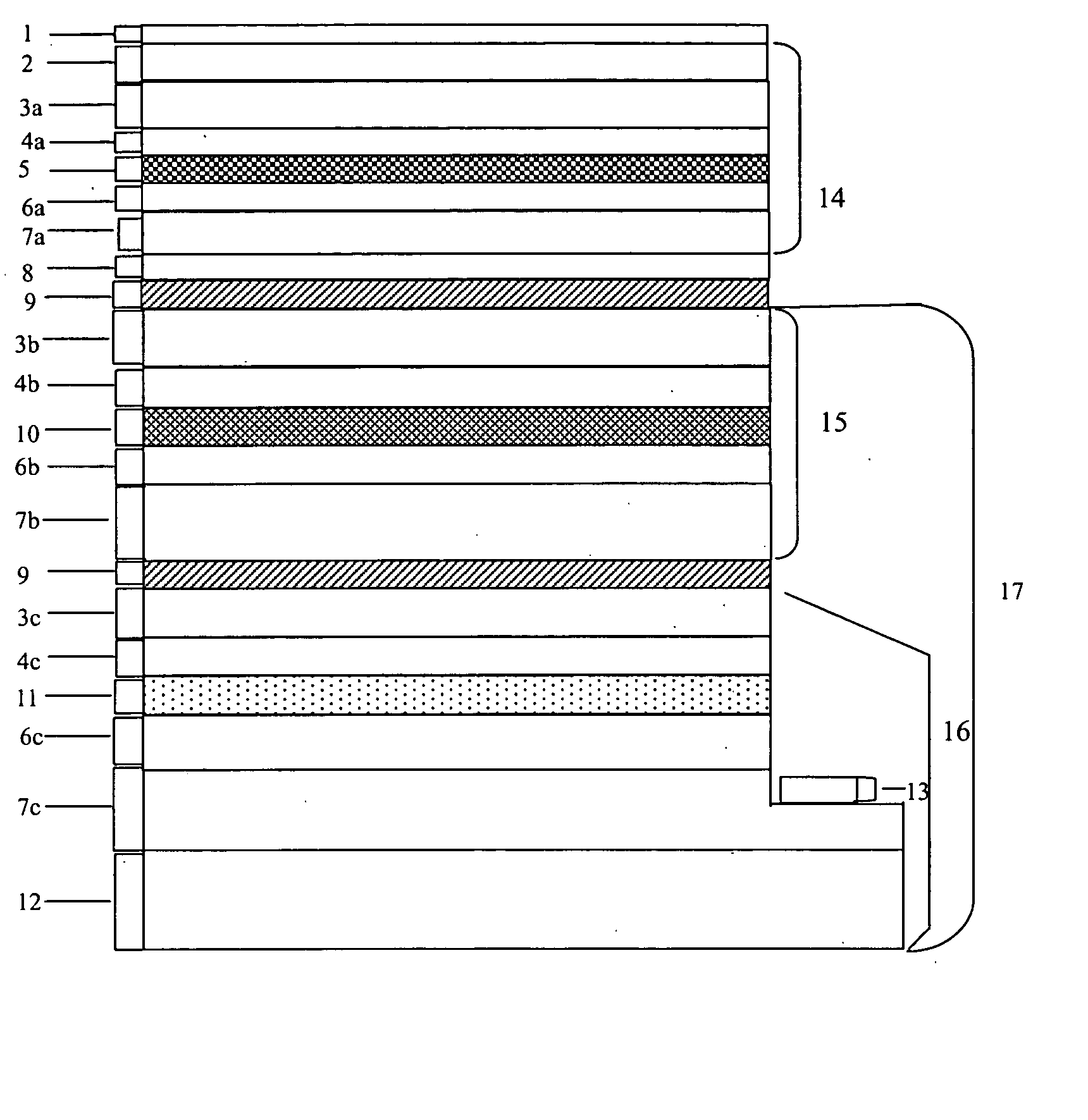
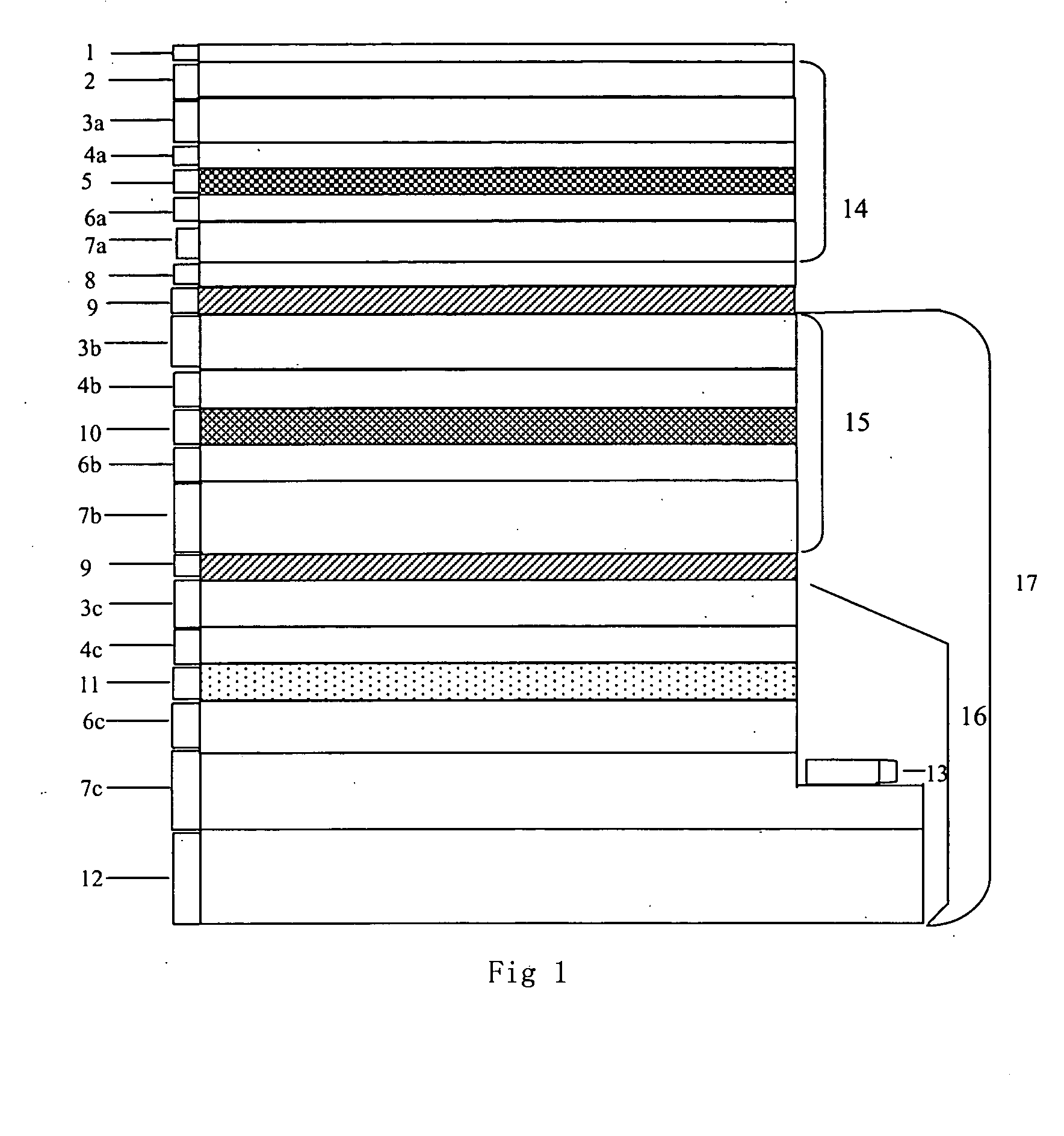
A high efficiency and high brightness multi-active layer tunneling regenerated white color semiconductor light emitting diode having a p type electrode 1, a monolithic red light cell 14, a tunnel junction 9, a monolithic green light 15 and blue light cell 16 (or a monolithic cyan light cell 19), wherein each of said cells are electrically connected by tunnel junctions 9, and the red cell physically connected with blue and green cell (or cyan cell) by wafer bonding layer 8. The lights from each cell synthesize white color light. The white light emitting diode only has one time optical-electrical conversion, so the quantum efficiency is high. Moreover, the white LED totally made from semiconductor materials, the lifetime of the white LED lamp is not limited by the relatively short lifetime of fluorescent material.
Owner:BEIJING UNIV OF TECH
Semiconductor light-emitting device
InactiveUS20050001227A1Improve external quantum efficiencyImprove efficiencySemiconductor/solid-state device detailsSolid-state devicesQuantum efficiencyCrystallographic defect
Owner:NICHIA CORP
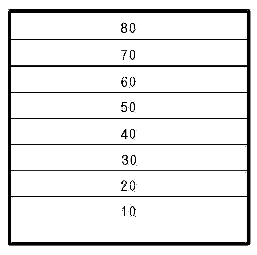
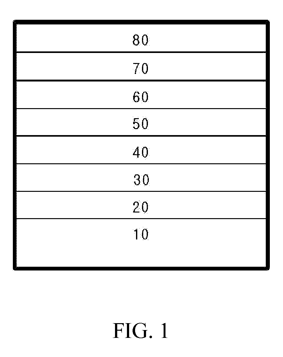
Quantum dot luminescent device
ActiveCN103904178APrevent spontaneous transferGuaranteed electrical neutralitySolid-state devicesSemiconductor/solid-state device manufacturingQuantum efficiencyCharge carrier
The invention provides a quantum dot luminescent device. The quantum dot luminescent device comprises an anode, a hole transport layer, a quantum dot luminescent layer, an electronic transfer layer and a cathode which are arranged sequentially and adjacently. The quantum dot luminescent device further comprises an electronic barrier layer. The electronic barrier layer is arranged in the electronic transfer layer or between the quantum dot luminescent layer and the electronic transfer layer. Due to the arrangement of the electronic barrier layer, balance injection of charge carriers is ensured, automatic charge transfer between the electronic transfer layer and the quantum dot luminescent layer is isolated, electric neutrality of a quantum dot is ensured, then the quantum dot luminescent device can keep deserved luminous efficiency, the external quantum efficiency of the quantum dot luminescent device is improved, and meanwhile the service life of the quantum dot luminescent device is largely prolonged.
Owner:ZHEJIANG UNIV +1
High fill factor multi-way shared pixel
ActiveUS20060256221A1Increases potential fill factorQuantum efficiencyTelevision system detailsTelevision system scanning detailsQuantum efficiencyFill factor
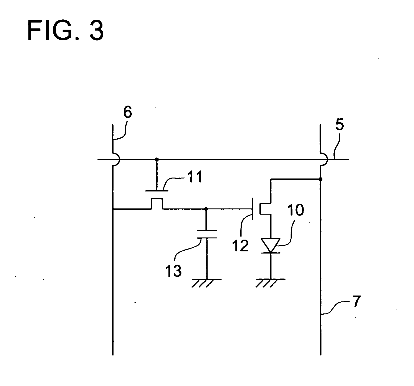
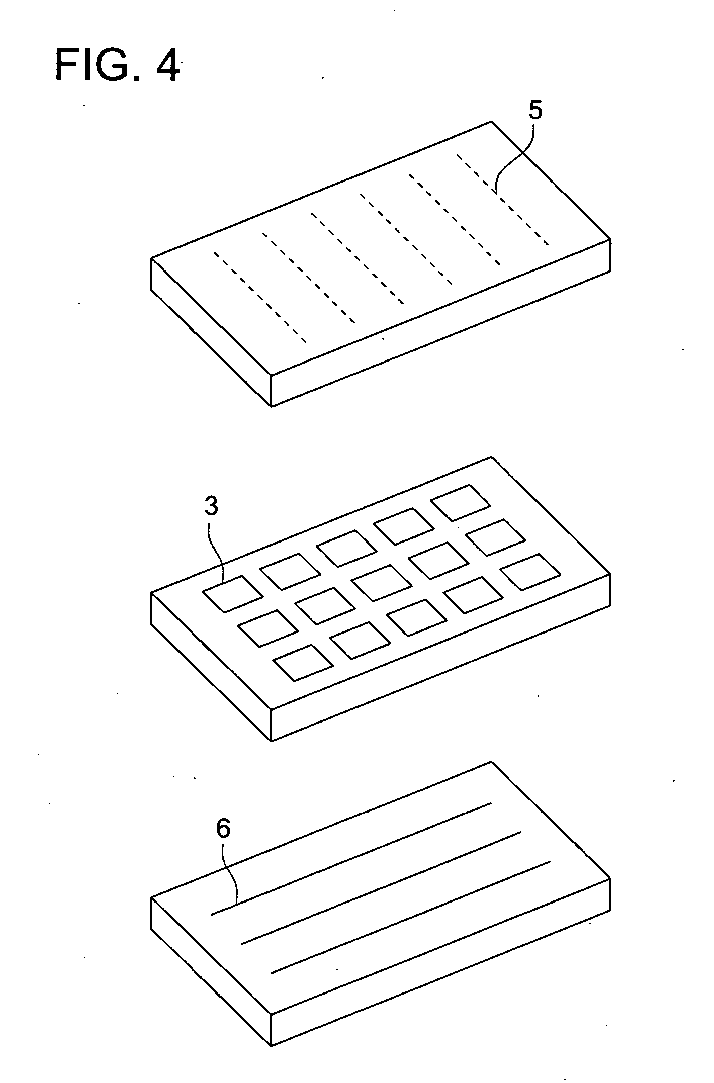
A pixel cell array architecture having a multiple pixel cells with shared pixel cell components. The individual pixel cell architecture increases the fill factor and the quantum efficiency for the pixel cell. The common pixel cell components may be shared by a number of pixels in the array, and may include several components that are associated with the readout of a signal from the pixel cell. Other examples of the pixel array architecture having improved fill factor for pixels in the array include an angled transfer gate and an efficiently located, shared capacitor.
Owner:APTINA IMAGING CORP
Light-emitting element
ActiveUS8853680B2Efficient formationReduce probabilitySolid-state devicesSemiconductor/solid-state device manufacturingQuantum efficiencyEngineering
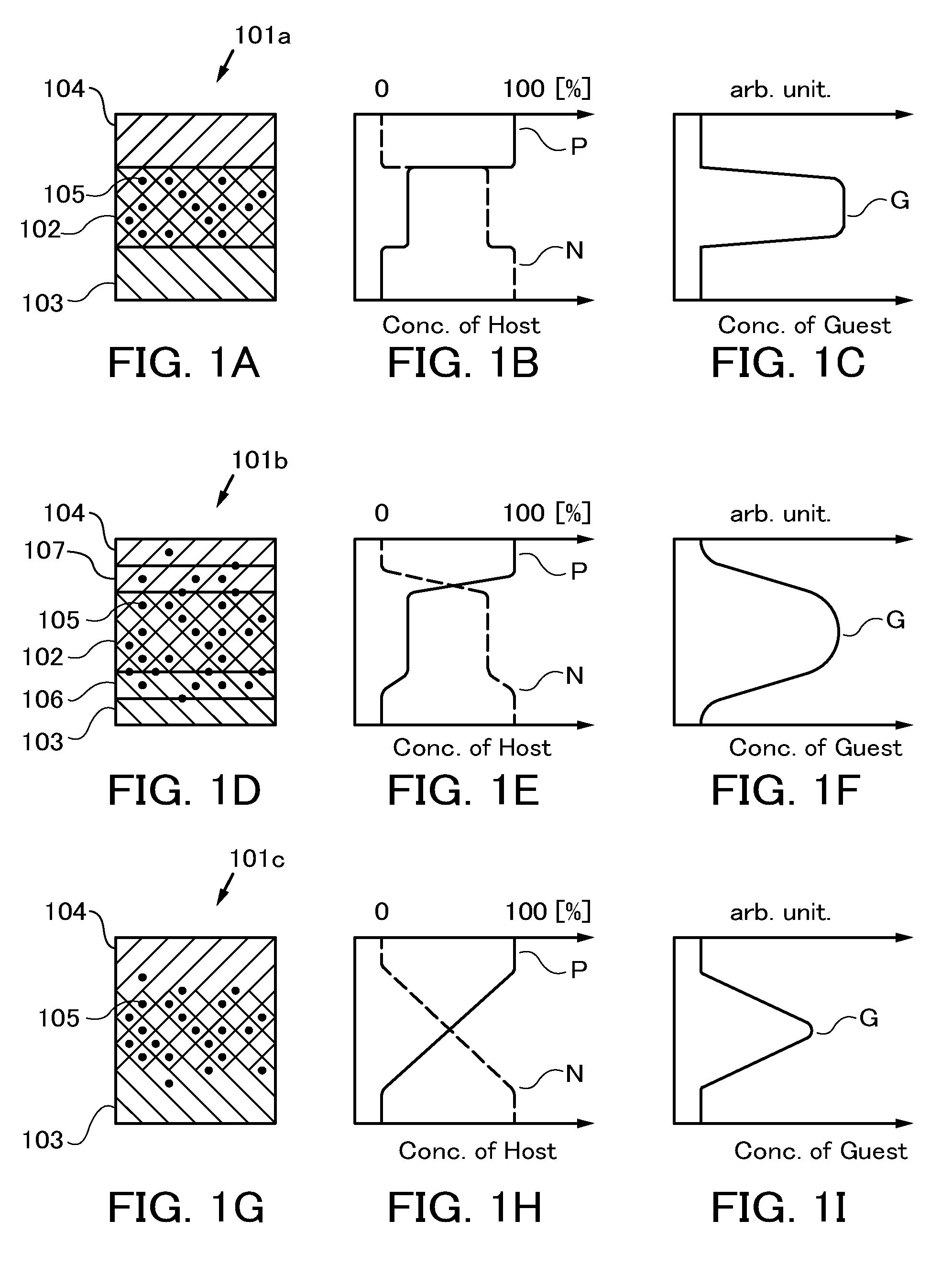
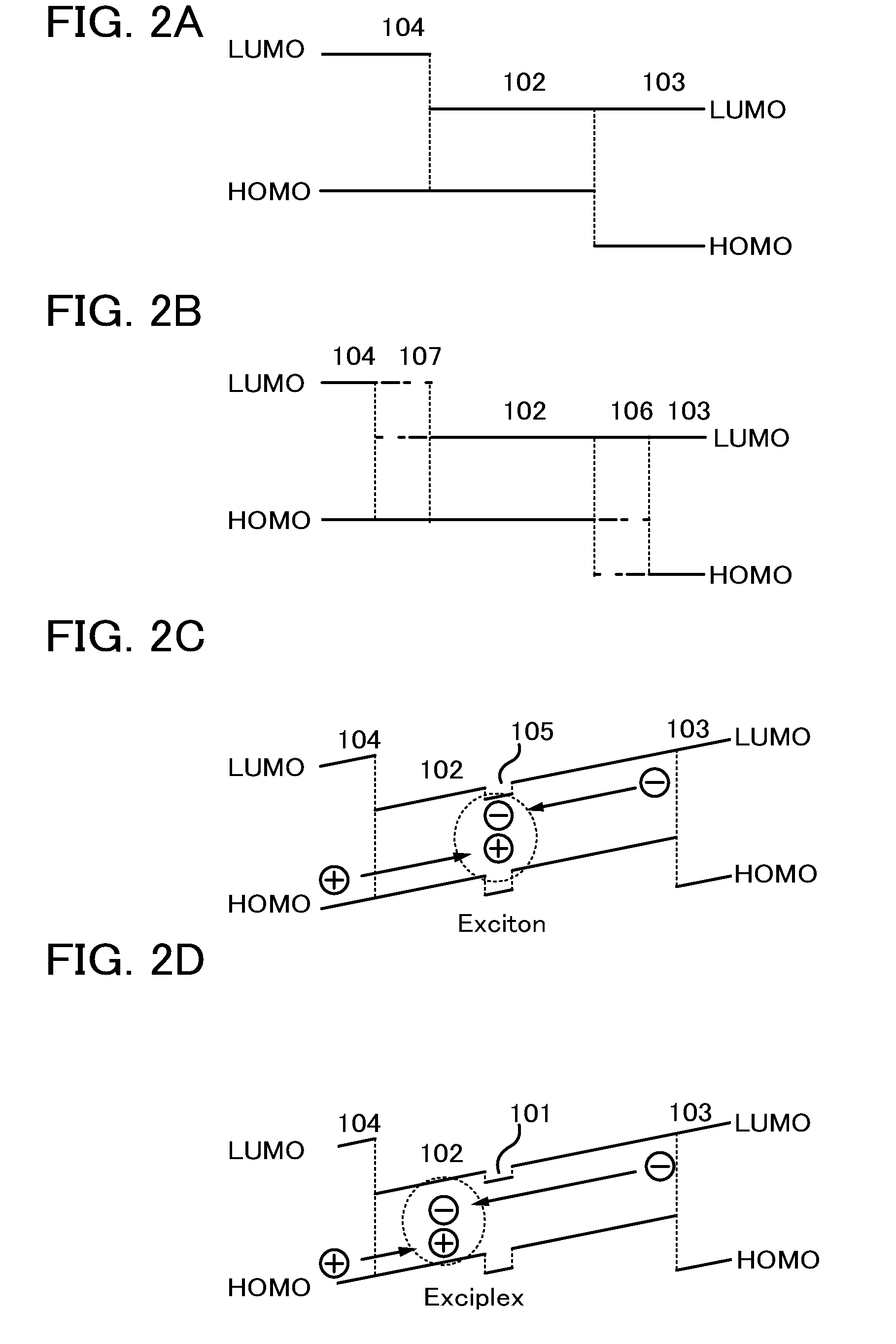
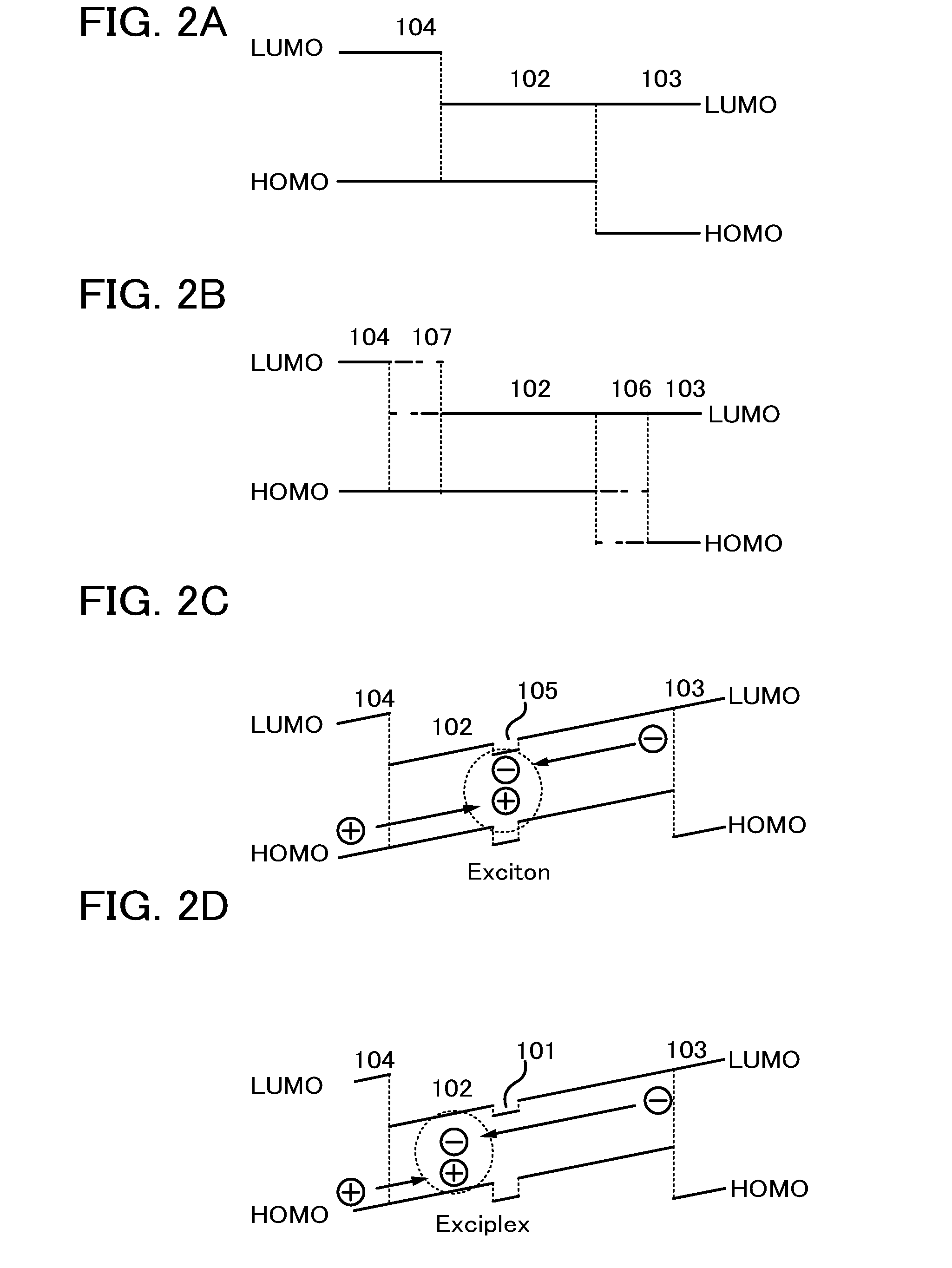
A light-emitting element having extremely high efficiency of approximately 25% is provided. The light-emitting element includes a light-emitting layer which contains a phosphorescent guest, an n-type host, and a p-type host, where the light-emitting layer is interposed between an n-type layer including the n-type host and a p-type layer including the p-type host, and where the n-type host and the p-type host are able to form an exciplex in the light-emitting layer. The light-emitting element exhibits an extremely high emission efficiency (power efficiency of 74.3 lm / W, external quantum efficiency of 24.5%, energy efficiency of 19.3%) at a low driving voltage (2.6 V) at which luminance of 1200 cd / m2 is attainable.
Owner:SEMICON ENERGY LAB CO LTD
OLEDs having increased external electroluminescence quantum efficiencies
InactiveUS7012363B2Discharge tube luminescnet screensElectroluminescent light sourcesQuantum efficiencyMicroparticle
OLED devices are disclosed having increased external electroluminescence quantum efficiencies, i.e., increased “out-coupling” efficiencies. OLED devices that have increased out-coupling efficiencies and that are also protected from environmental elements such as moisture and oxygen are also disclosed. The OLED device of the present invention comprises a substrate; an active region positioned on the substrate, wherein the active region comprises an anode layer, a cathode layer and a light-emitting layer disposed between the anode layer and the cathode layer; and a polymeric layer disposed (a) over the active region, (b) under the active region or (c) both over and under the active region. The polymeric layer has microparticles incorporated therein, and the microparticles are effective to increase the out-coupling efficiency of the OLED. In one embodiment, the OLED device comprises a composite barrier layer and the microparticles are incorporated in a polymeric planarizing sublayer of the composite barrier layer. The composite barrier layer in this embodiment also protects the OLED from damage caused by environmental elements such as moisture and / or oxygen.
Owner:UNIVERSAL DISPLAY
Light-emitting element
ActiveUS20120248421A1Efficient formationReduce probabilitySolid-state devicesSemiconductor/solid-state device manufacturingQuantum efficiencyEngineering
A light-emitting element having extremely high efficiency of approximately 25% is provided. The light-emitting element includes a light-emitting layer which contains a phosphorescent guest, an n-type host, and a p-type host, where the light-emitting layer is interposed between an n-type layer including the n-type host and a p-type layer including the p-type host, and where the n-type host and the p-type host are able to form an exciplex in the light-emitting layer. The light-emitting element exhibits an extremely high emission efficiency (power efficiency of 74.3 lm / W, external quantum efficiency of 24.5%, energy efficiency of 19.3%) at a low driving voltage (2.6 V) at which luminance of 1200 cd / m2 is attainable.
Owner:SEMICON ENERGY LAB CO LTD
Functionalized matrices for dispersion of nanostructures
ActiveUS8283412B2Good miscibilityInhibit aggregationMaterial nanotechnologyGroup 4/14 element organic compoundsAnti-reflective coatingSemiconductor nanocrystals
Matrixes doped with semiconductor nanocrystals are provided. In certain embodiments, the semiconductor nanocrystals have a size and composition such that they absorb or emit light at particular wavelengths. The nanocrystals can comprise ligands that allow for mixing with various matrix materials, including polymers, such that a minimal portion of light is scattered by the matrixes. The matrixes are optionally formed from the ligands. The matrixes of the present invention can also be utilized in refractive index matching applications. In other embodiments, semiconductor nanocrystals are embedded within matrixes to form a nanocrystal density gradient, thereby creating an effective refractive index gradient. The matrixes of the present invention can also be used as filters and antireflective coatings on optical devices and as down-converting layers. Processes for producing matrixes comprising semiconductor nanocrystals are also provided. Nanostructures having high quantum efficiency, small size, and / or a narrow size distribution are also described, as are methods of producing indium phosphide nanostructures and core-shell nanostructures with Group II-VI shells.
Owner:SHOEI CHEM IND CO LTD
Authenticating and identifying objects using markings formed with correlated random patterns
InactiveUS20080138604A1Layered productsRecord carriers used with machinesQuantum efficiencyPhotoluminescence
Described herein are techniques for authenticating and identifying objects using markings formed with correlated random patterns. In one embodiment, an object to be authenticated includes a substrate and a marking adjacent to the substrate. The marking includes a luminescent material distributed in accordance with a correlated random pattern, and the luminescent material exhibits photoluminescence having a quantum efficiency of at least 10 percent.
Owner:OMNIPV
Solid-state imaging device, camera and method of producing the solid-state imaging device
InactiveUS20060006488A1High sensitivityInhibit currentTelevision system detailsSolid-state devicesQuantum efficiencyInterconnection
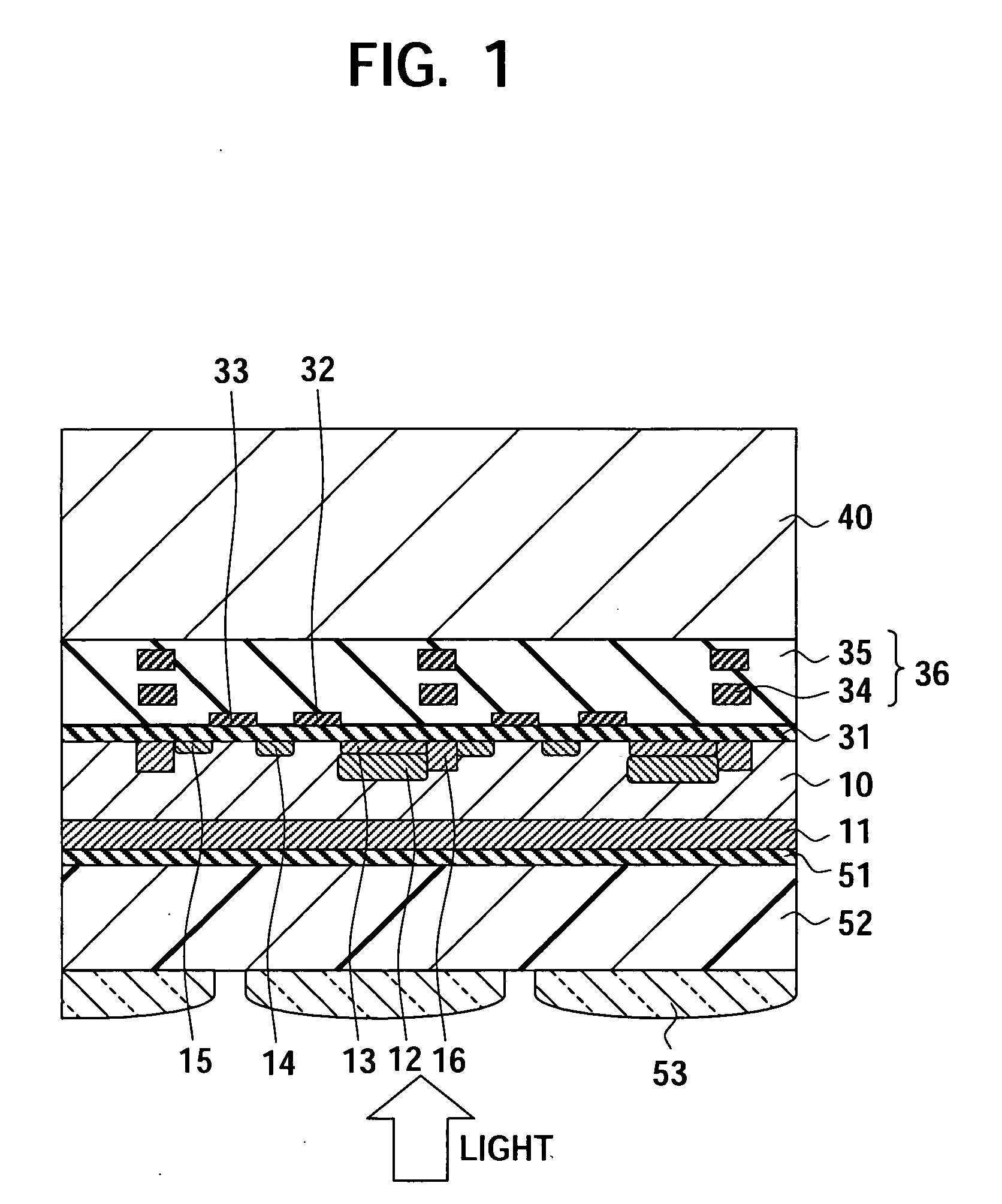
To provide a back-illuminated solid-state imaging device able to suppress a crystal defect caused by a metal contamination in a process and to suppress a dark current to improve quantum efficiency, a camera including the same and a method of producing the same, having the steps of forming a structure including a substrate, a first conductive type epitaxial layer and a first conductive type impurity layer, the first conductive type epitaxial layer being formed on the substrate to have a first impurity concentration, and the first conductive type impurity layer being formed in a boundary region to have a second impurity concentration higher than the first impurity concentration of the epitaxial layer; forming a second conductive type region storing a charge generated by a photoelectric conversion in the epitaxial layer; forming an interconnection layer on the epitaxial layer; and removing the substrate.
Owner:SONY CORP
Fabrication method of nitride-based semiconductors and nitride-based semiconductor fabricated thereby
ActiveUS6844569B1Reduce dislocationReduce stressPolycrystalline material growthSolid-state devicesQuantum efficiencyMetal clusters
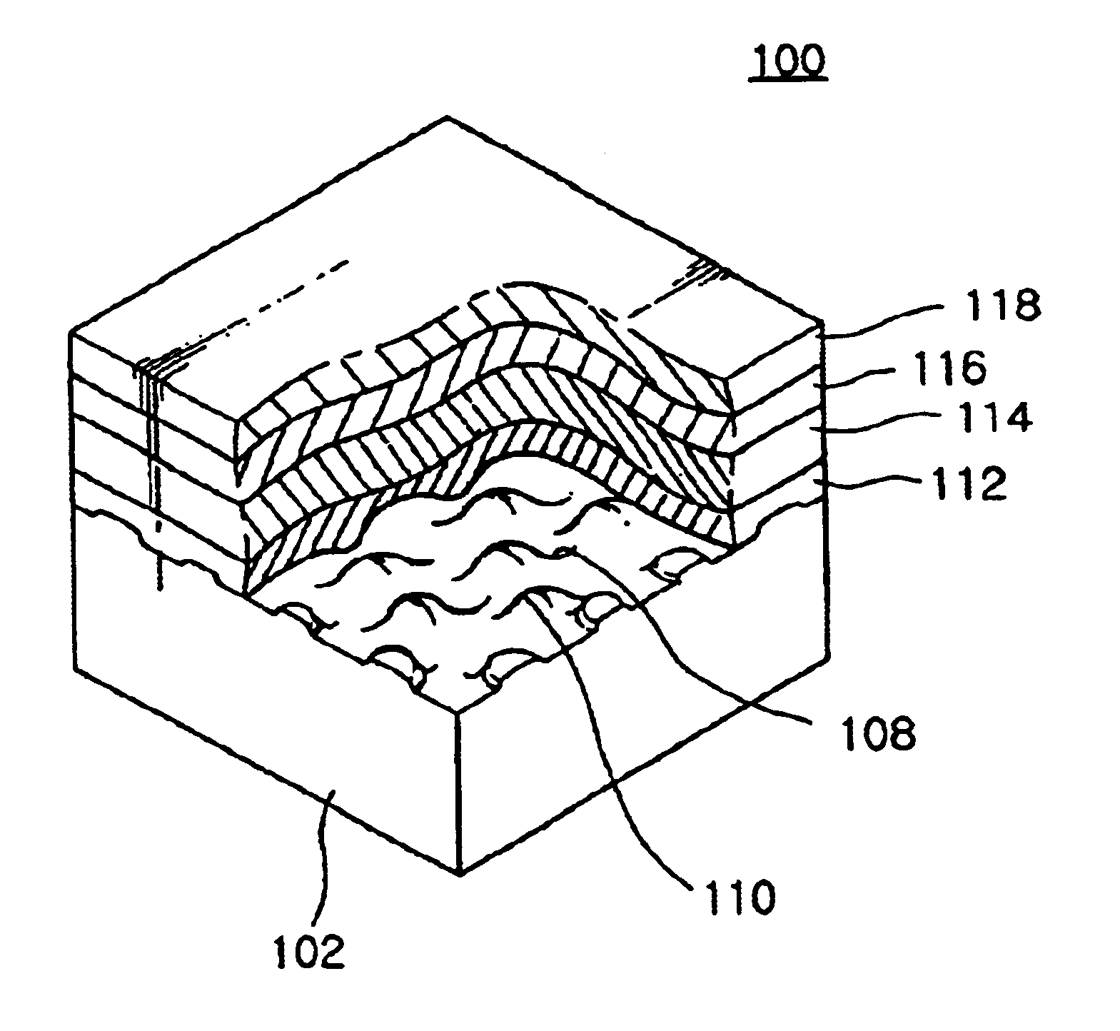
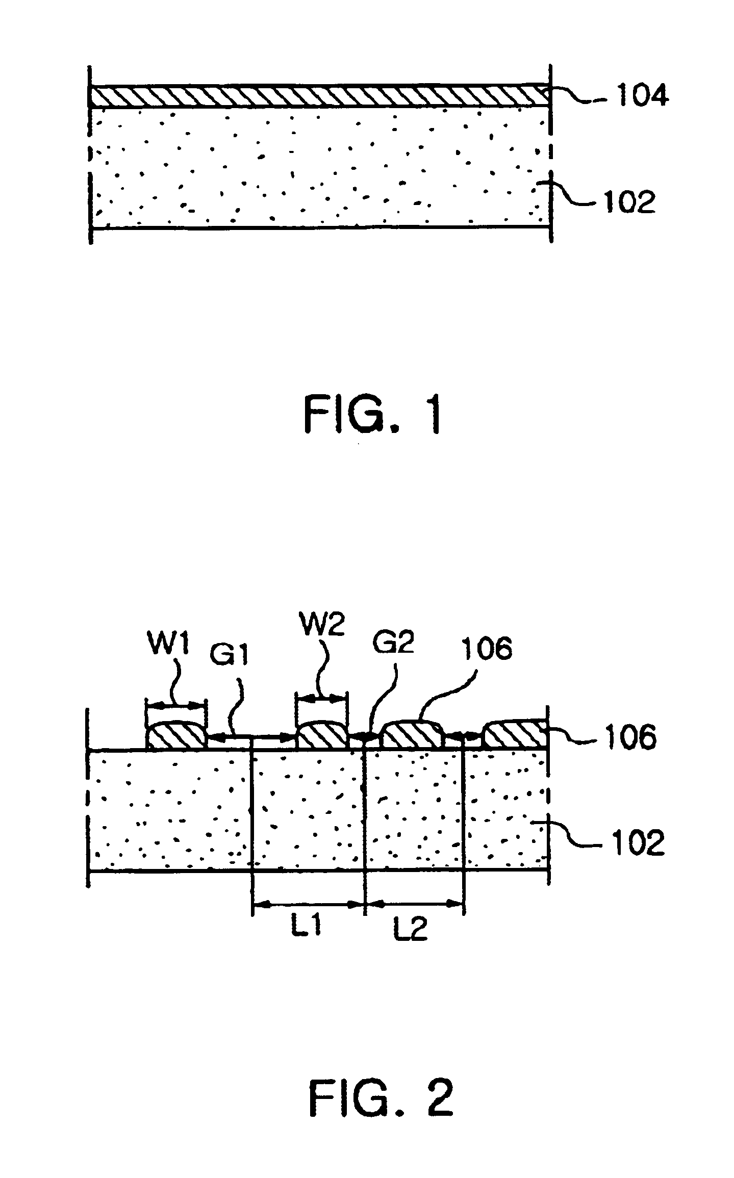
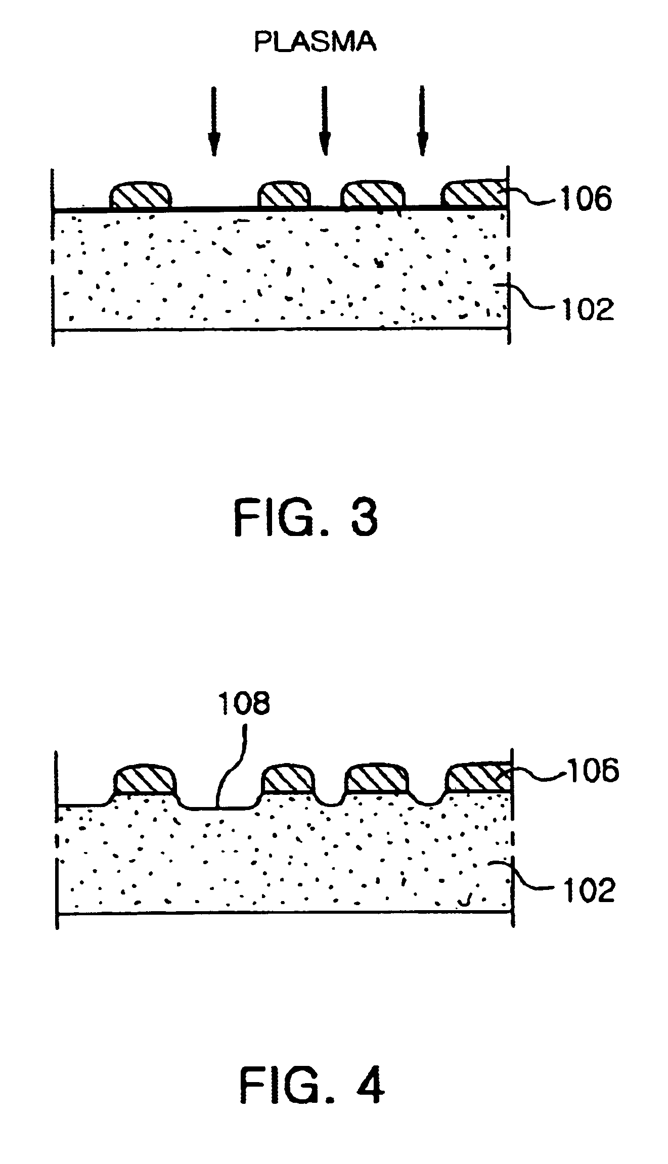
The present invention relates to a fabrication method of nitride-based semiconductors and a nitride-based semiconductor fabricated thereby. In the fabrication method of the invention, a self-organizing metal layer is formed on a sapphire substrate. The sapphire substrate having the self-organizing metal layer is heated so that self-organizing metal coalesces into nanoscale clusters to irregularly expose an upper surface of the sapphire substrate. Exposed portions of the sapphire substrate is plasma etched using the self-organized metal clusters as a mask to form a nanoscale uneven structure on the sapphire substrate. A resultant structure is wet etched to remove the self-organized metal clusters. The nanoscale uneven structure formed on the sapphire substrate decreases the stress and resultant dislocation between the sapphire substrate and a nitride-based semiconductor layer as well as increases the quantum efficiency between the same.
Owner:SAMSUNG ELECTRONICS CO LTD
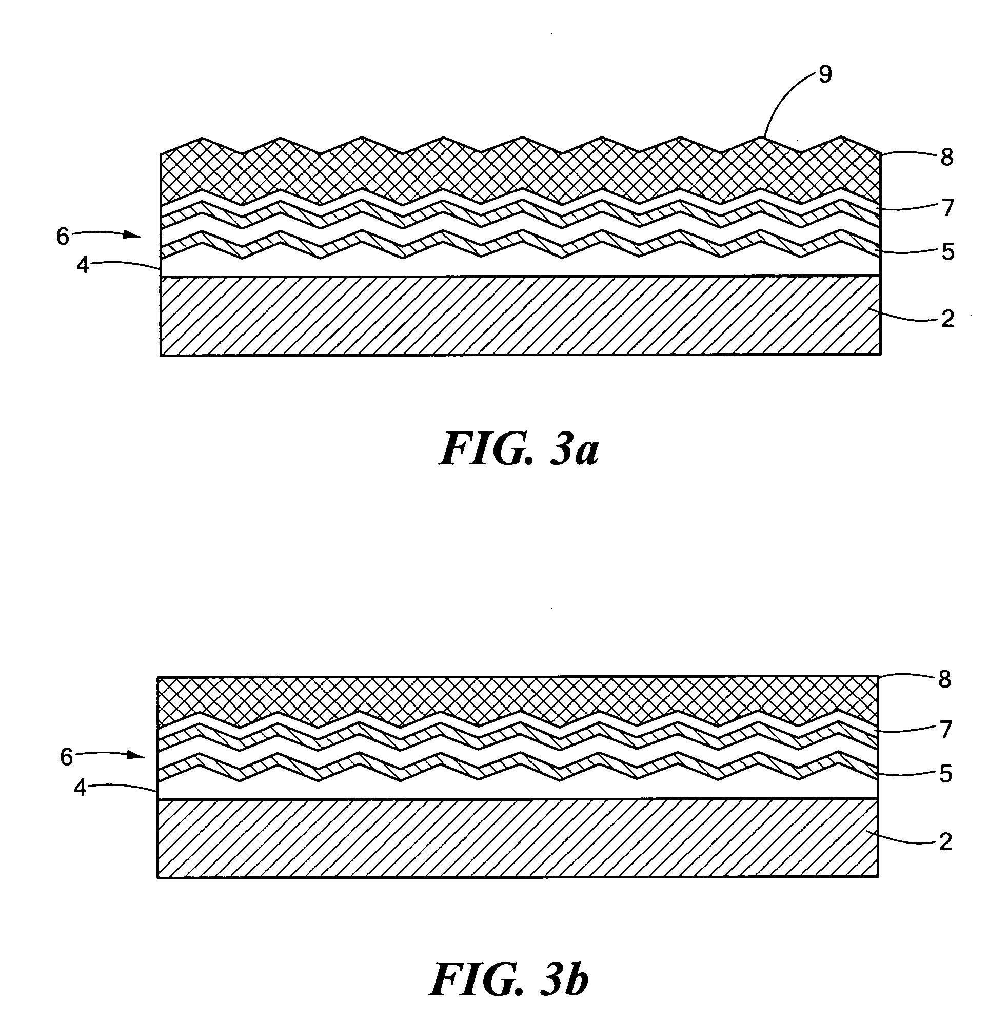
Front electrode including transparent conductive coating on patterned glass substrate for use in photovoltaic device and method of making same
InactiveUS20080178932A1Reduced visible light reflectionImprove conductivitySemiconductor/solid-state device manufacturingPhotovoltaic energy generationPeak valuePeak area
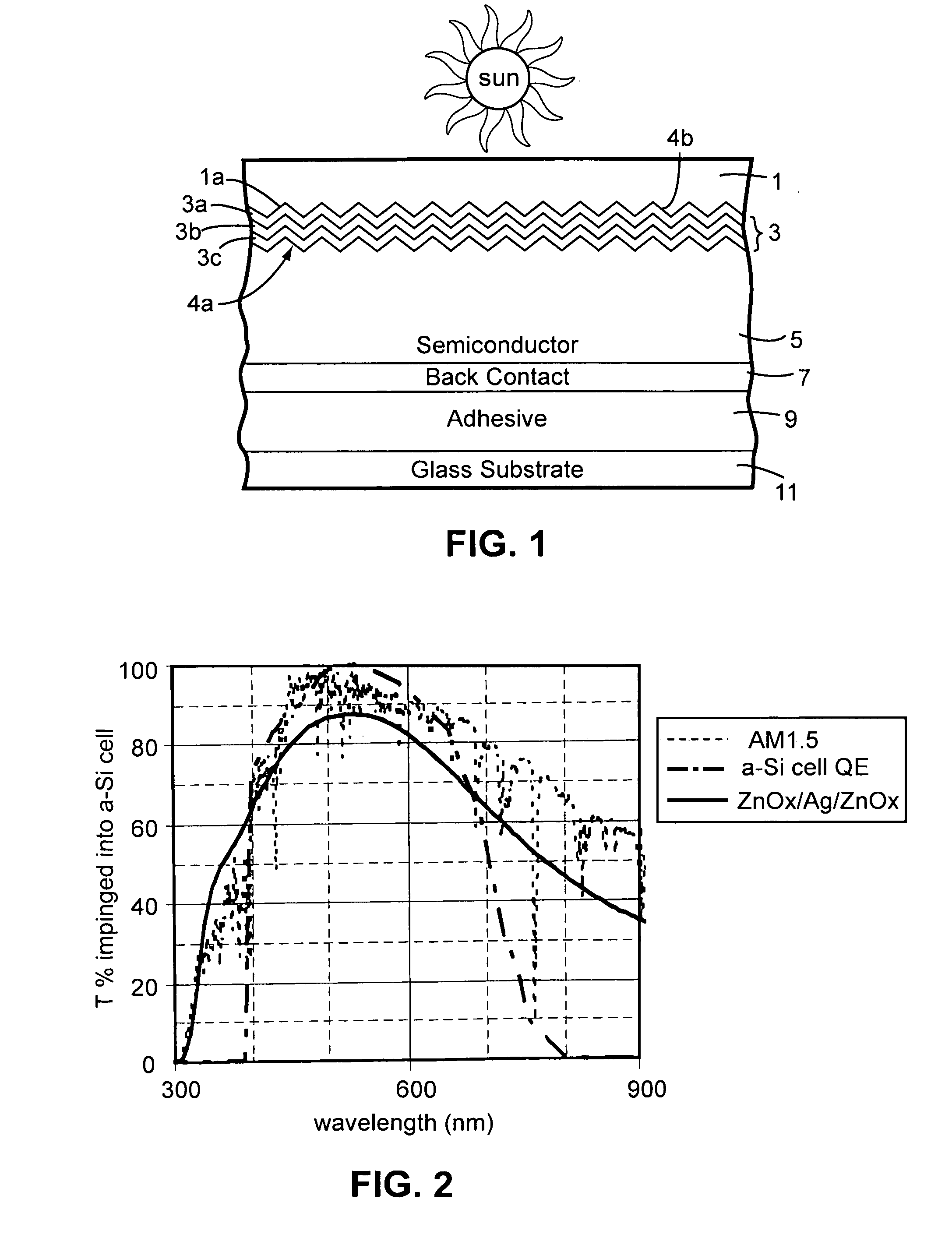
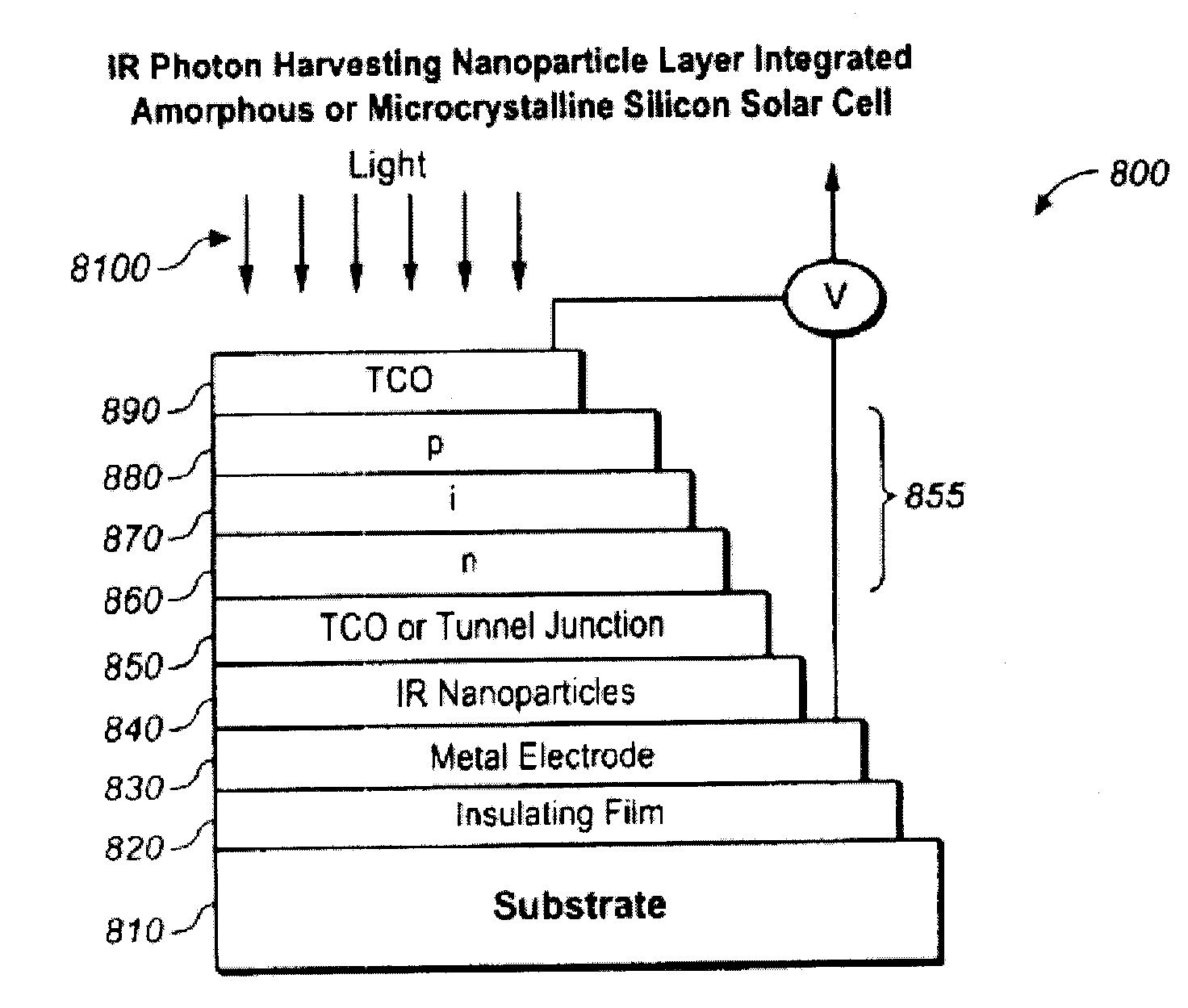
This invention relates to a photovoltaic device including an electrode such as a front electrode / contact. In certain example embodiments, the front electrode of the photovoltaic device includes a multi-layered transparent conductive coating which is sputter-deposited on a textured surface of a patterned glass substrate. In certain example embodiments, a maximum transmission area of the substantially transparent conductive front electrode is located under a peak area of a quantum efficiency (QE) and / or QEx (photon flux of solar radiation) curve of the photovoltaic device and a light source spectrum used to power the photovoltaic device. In certain example embodiments, the front electrode includes a transparent conductive layer of or including one or more of (i) titanium zinc oxide doped with aluminum and / or niobium, and / or (ii) titanium niobium oxide.
Owner:GUARDIAN GLASS LLC
All-fiber photon-pair source for quantum communications
ActiveUS6897434B1Improve quantum efficiencyLimit dark count rateOptical radiation measurementMirrorsHigh rateDark count rate
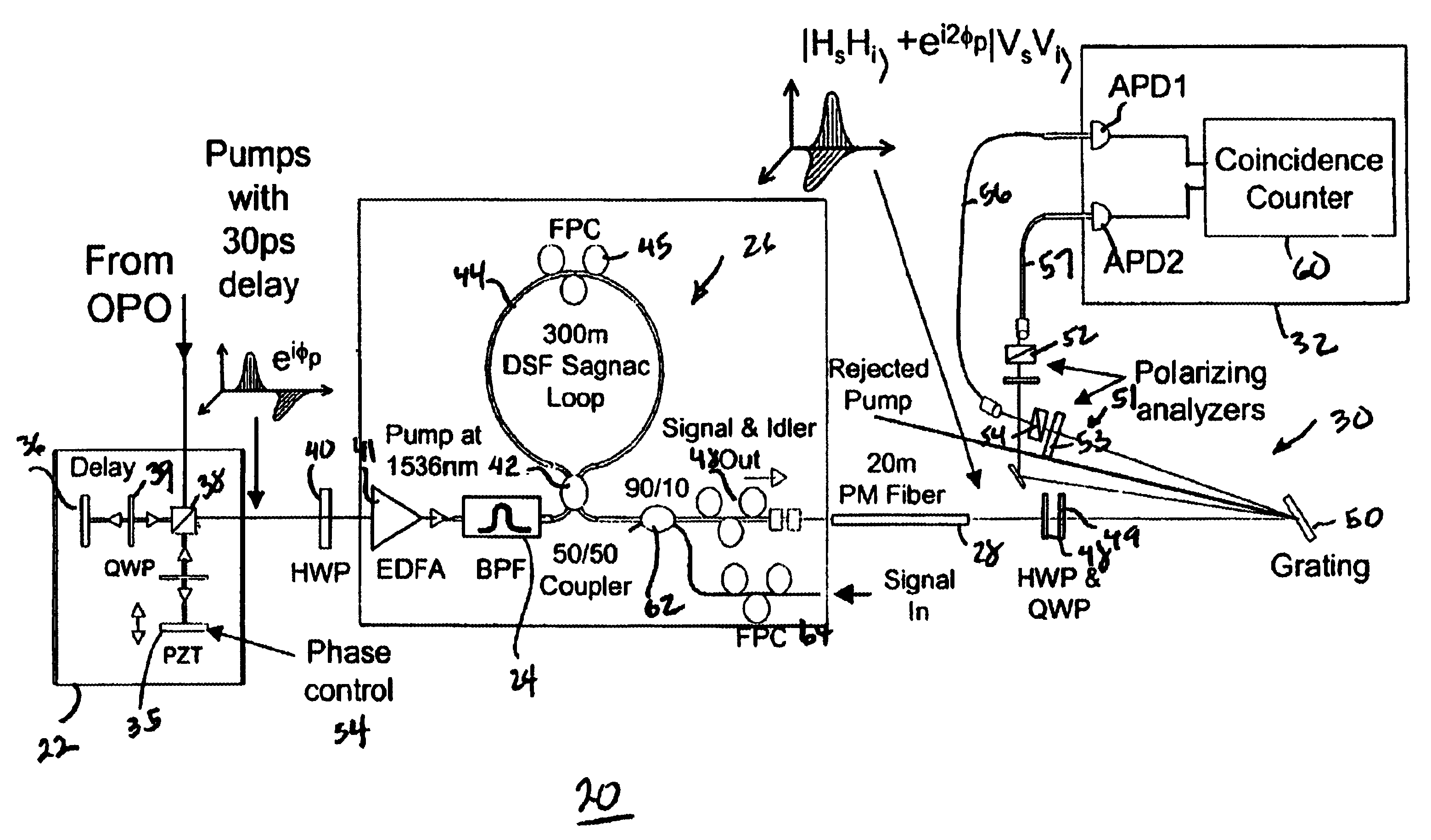
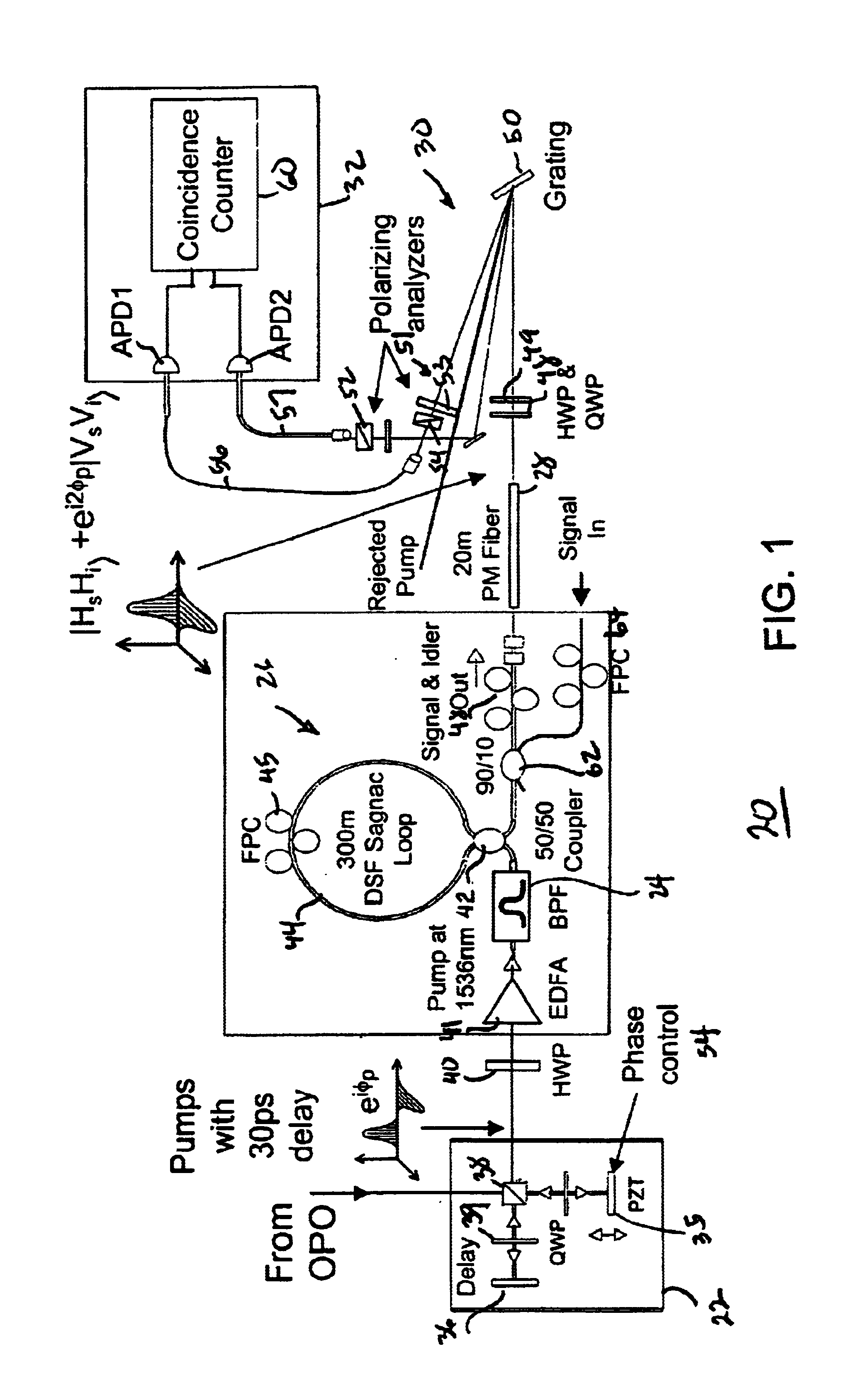
A source and / or method of generating quantum-correlated and / or entangled photon pairs using parametric fluorescence in a fiber Sagnac loop. The photon pairs are generated in the 1550 nm fiber-optic communication band and detected by a detection system including InGaAs / InP avalanche photodiodes operating in a gated Geiger mode. A generation rate>103 pairs / s is observed, a rate limited only by available detection electronics. The nonclassical nature of the photon correlations in the pairs is demonstrated. This source, given its spectral properties and robustness, is well suited for use in fiber-optic quantum communication and cryptography networks. The detection system also provides high rate of photon counting with negligible after pulsing and associated high quantum efficiency and also low dark count rate.
Owner:NORTHWESTERN UNIV
Carbon nano-dot, and preparation method and application thereof
ActiveCN102849722AOvercome costsOvercoming the problem of easy fluorescence quenching in the aggregated stateNanotechnologyNano-carbonBiological imagingOrganic compound
The invention discloses a carbon nano-dot, and a preparation method and an application thereof, and solves a problem that the application of present nano-dots is restricted because of high preparation cost and easy fluorescent quenching appearance of an aggregate state. According to the invention, the carbon nano-dot having a high fluorescence quantum efficiency is prepared through adopting a polycarboxyl or polyhydroxy contained organic compound, or an amino acid as a raw material, and urea as a surface passivation modification agent, and through a microwave process, and a carbon nano-dot fluorescent ink is prepared through using the carbon nano-dot. The preparation method disclosed in the invention has the advantages of simplicity, low cost and convenient large-scale production; the fluorescent quenching of the prepared carbon nano-dot on the surface of a biological product does not appear, and the highest fluorescence quantum efficiency is 42%; and the prepared carbon nano-dot fluorescent ink is nontoxic, does not generate a precipitate after long-time dispose, and can be applied to the biological imaging field, the biological product identification field, the information storage field, the information encryption field, the false proof field, the illumination display field, the photovoltaic device field and the like.
Owner:CHANGCHUN INST OF OPTICS FINE MECHANICS & PHYSICS CHINESE ACAD OF SCI
Optical devices featuring textured semiconductor layers
InactiveUS20050242364A1Light extraction efficiencyEfficient couplingSemiconductor/solid-state device manufacturingNanoopticsQuantum efficiencySolar cell
A semiconductor sensor, solar cell or emitter or a precursor therefore having a substrate and textured semiconductor layer deposited onto the substrate. The layer can be textured as grown on the substrate or textured by replicating a textured substrate surface. The substrate or first layer is then a template for growing and texturing other semiconductor layers from the device. The textured layers are replicated to the surface from the substrate to enhance light extraction or light absorption. Multiple quantum wells, comprising several barrier and quantum well layers, are deposited as alternating textured layers. The texturing in the region of the quantum well layers greatly enhances internal quantum efficiency if the semiconductor is polar and the quantum wells are grown along the polar direction. This is the case in nitride semiconductors grown along the polar [0001] or [000-1] directions.
Owner:TRUSTEES OF BOSTON UNIV
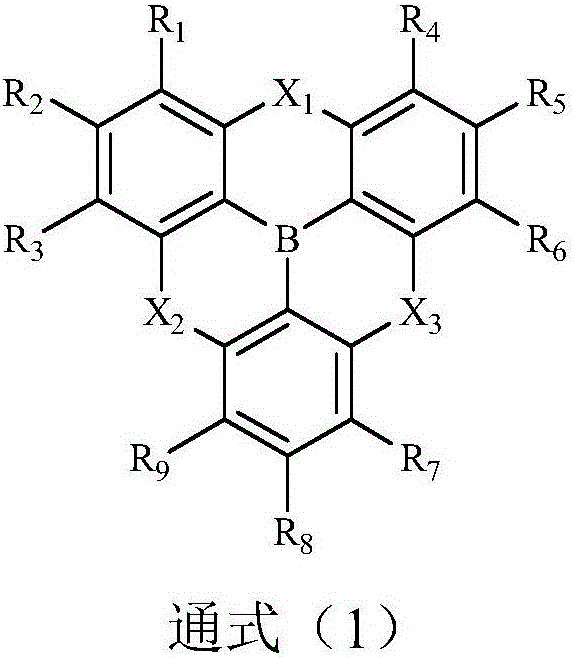
Boron-containing organic electroluminescent compound and application to OLED device
ActiveCN106467553AImprove applicabilityImprove luminous efficiencySolid-state devicesSemiconductor/solid-state device manufacturingFluorescenceStructural formula
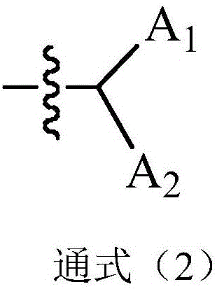
The invention discloses a boron-containing efficient organic electroluminescent compound and application of the compound to an OLED device. The structural formula of the compound is as shown in the general formula (1). Boron atom as the core extends outward three six-membered rings composed of carbon-carbon single bonds, wherein the carbon-carbon single bonds also can be replaced with carbon-oxygen and carbon-nitrogen bonds; a benzene ring is sandwiched between each two six-membered rings; and each phenyl ring is respectively externally connected to hydrogen, aryl group, heteroaryl group, alkyl group, alkyloxy group, or arylamine group. The material has good fluorescence quantum efficiency and electroluminescent efficiency, is easy to form an amorphous film, and has good heat stability. Thus, the material can be used as a luminescent layer material in an organic electroluminescent device.
Owner:JIANGSU SUNERA TECH CO LTD
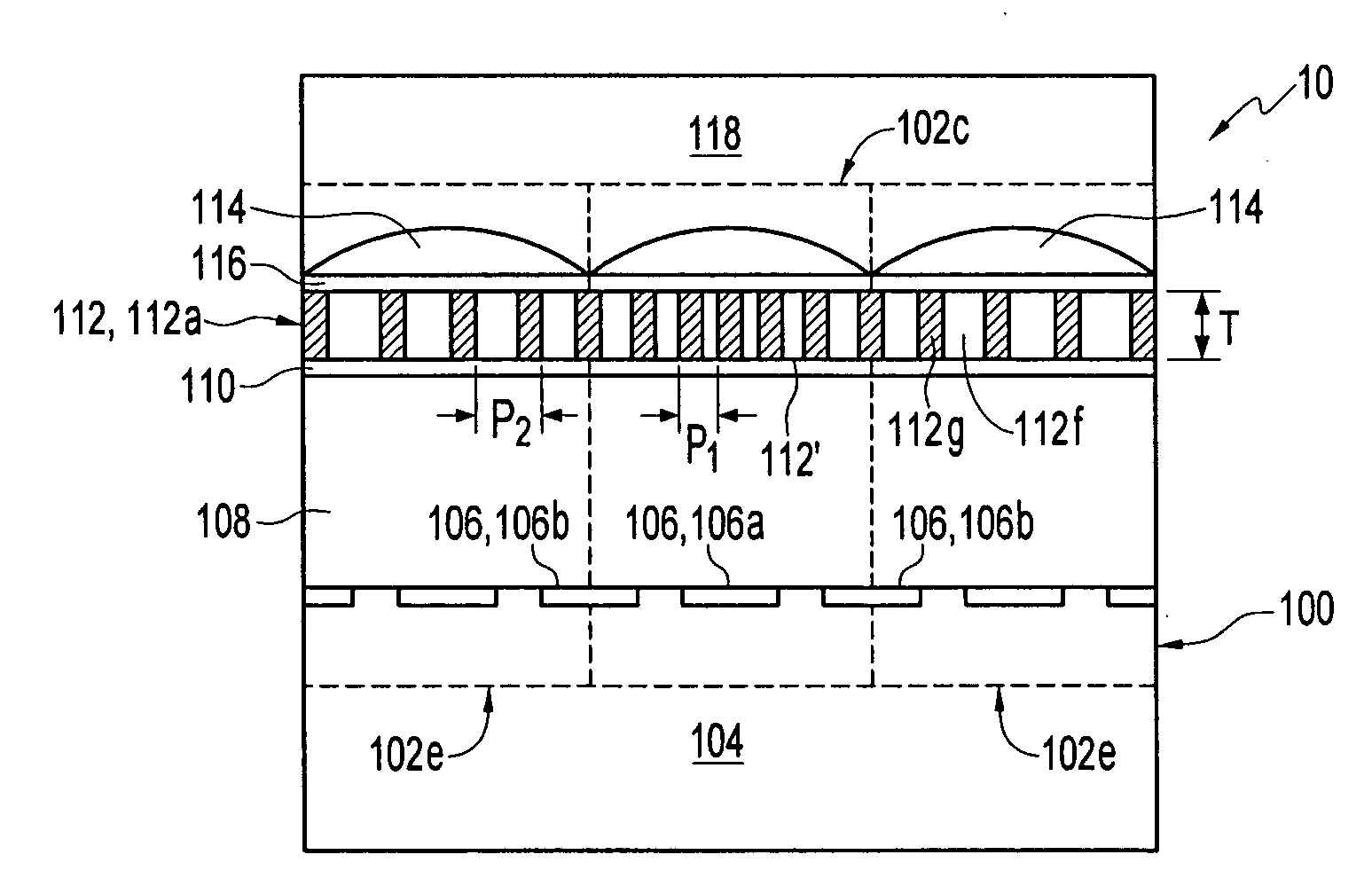
Method and apparatus providing imager pixel array with grating structure and imager device containing the same
ActiveUS20070298533A1Solid-state devicesSemiconductor/solid-state device manufacturingQuantum efficiencyGrating
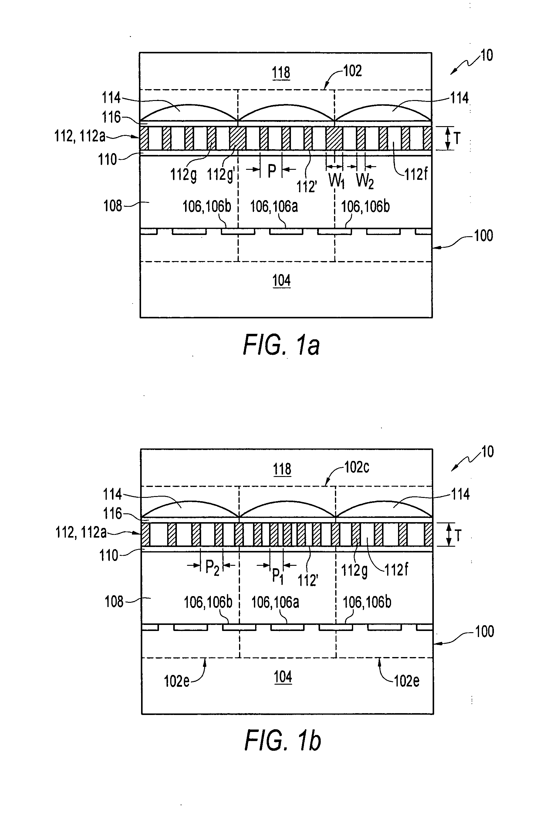
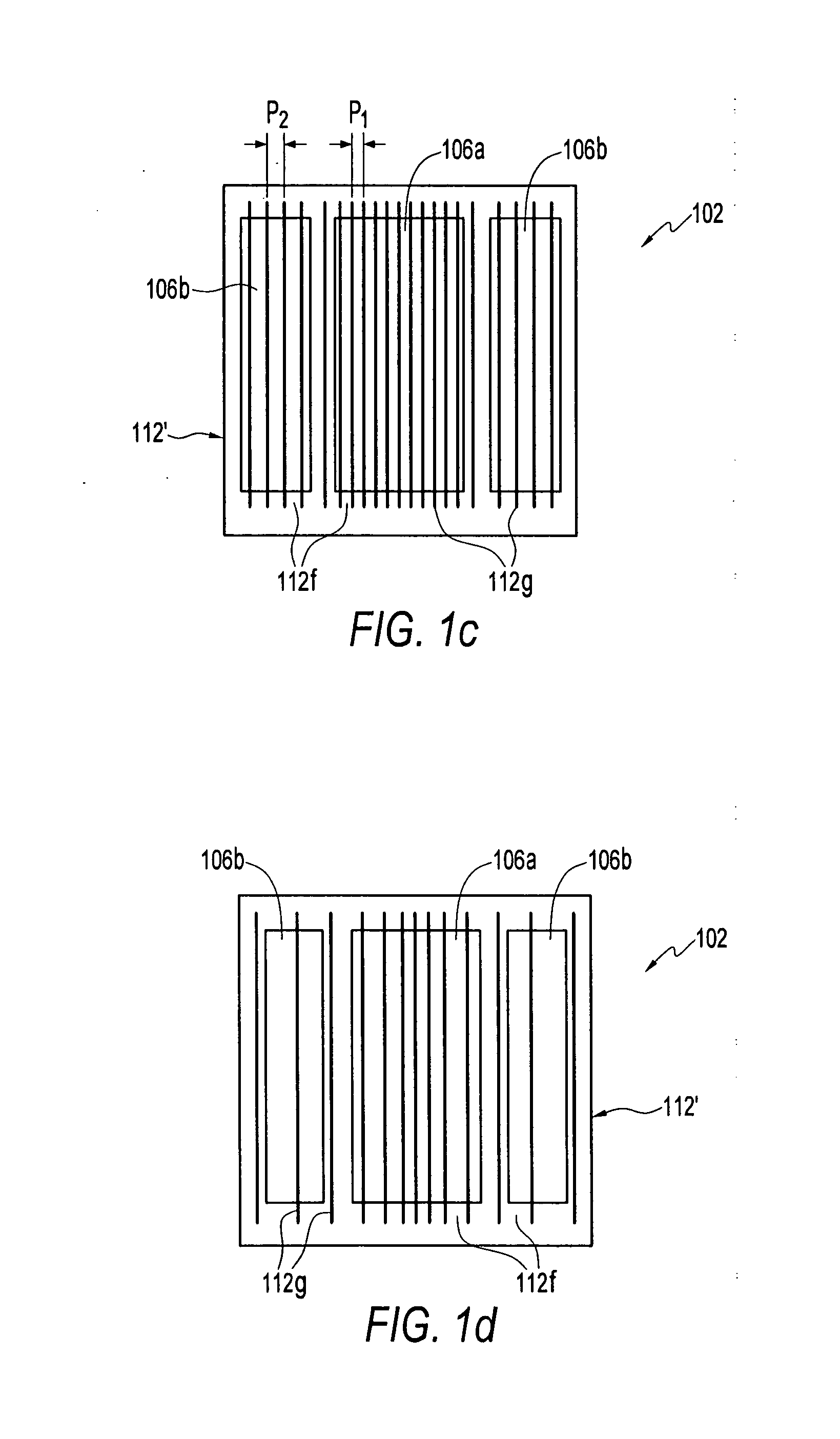
An imager pixel array capable of separating and detecting the spectral components of an incident light without the use of a color filter array. The imager pixel array employs a grating layer which allows one or more spectral components of incident light to be transmitted therethrough, but diffracts other spectral components of the incident light. Both the transmitted and diffracted spectral components can be sensed by photosensors in the imager pixel array and used in subsequent data processing, thereby improving the quantum efficiency of the imager device. The grating layer can be formed of first and second materials each having a refractive index which are substantially the same at a predetermined wavelength.
Owner:APTINA IMAGING CORP
Nitride semiconductor light emitting element
InactiveUS20070122994A1Suppresses minimizesImprove film qualityLaser detailsSolid-state devicesThreading dislocationsQuantum efficiency
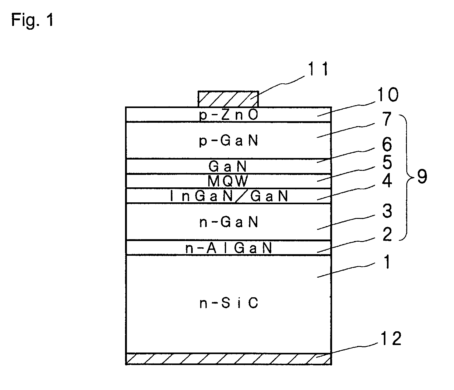
A nitride semiconductor light-emitting element suppresses leakage currents and non-radiative recombination centers by providing, as an underlying layer of the active layer, a pit formation layer that reliably generates pits, while maintaining a good film quality, so that the internal quantum efficiency is improved, and the light-emitting characteristics are also improved. A nitride semiconductor lamination portion including at least an active layer for forming a light-emitting portion is present on a substrate, and a pit formation layer is formed as a superlattice layer of nitride semiconductor on the side of the substrate of the active layer. The pit formation layer generates pits in the end portions of threading dislocations that are generated in the nitride semiconductor layer on the side of the substrate.
Owner:ROHM CO LTD
Quantum dots of group IV semiconductor materials
InactiveUS7358525B2NanoinformaticsSemiconductor/solid-state device manufacturingQuantum efficiencySemiconductor materials
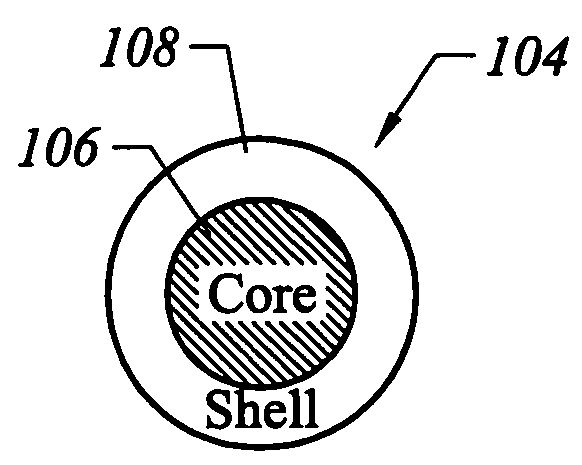
The invention relates to a quantum dot. The quantum dot comprises a core including a semiconductor material Y selected from the group consisting of Si and Ge. The quantum dot also comprises a shell surrounding the core. The quantum dot is substantially defect free such that the quantum dot exhibits photoluminescence with a quantum efficiency that is greater than 10 percent.
Owner:SAMSUNG ELECTRONICS CO LTD
Fluorescent substance and light-emitting device employing the same
ActiveUS20100025632A1Improve quantum efficiencyHigh emission intensitySolid-state devicesLuminescent compositionsQuantum efficiencyFluorescence
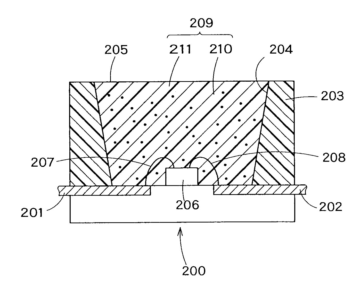
The present invention provides a fluorescent substance excellent both in quantum efficiency and in temperature characteristics, and also provides a light-emitting device utilizing the fluorescent substance. This fluorescent substance contains an inorganic compound comprising a metal element M, a trivalent element M1 other than the metal element M, a tetravalent element M2 other than the metal element M, and either or both of O and N. In the inorganic compound, the metal element M is partly replaced with a luminescence center element R. The crystal structure of the fluorescent substance is basically the same as Sr3Al3Si13O2N21, but the chemical bond lengths of M1-N and M2-N are within the range of ±15% based on those of Al—N and Si—N calculated from the lattice constants and atomic coordinates of Sr3Al3Si13O2N21, respectively. The fluorescent substance emits luminescence having a peak in the range of 490 to 580 nm when excited with light of 250 to 500 nm.
Owner:KK TOSHIBA
Who we serve
- R&D Engineer
- R&D Manager
- IP Professional
Why Patsnap Eureka
- Industry Leading Data Capabilities
- Powerful AI technology
- Patent DNA Extraction
Social media
Patsnap Eureka Blog
Learn More Browse by: Latest US Patents, China's latest patents, Technical Efficacy Thesaurus, Application Domain, Technology Topic, Popular Technical Reports.
© 2024 PatSnap. All rights reserved.Legal|Privacy policy|Modern Slavery Act Transparency Statement|Sitemap|About US| Contact US: [email protected]


