US7881010B2 - Process for self-aligned flare point and shield throat definition prior to main pole patterning - Google Patents
Process for self-aligned flare point and shield throat definition prior to main pole patterning Download PDFInfo
- Publication number
- US7881010B2 US7881010B2 US11/956,277 US95627707A US7881010B2 US 7881010 B2 US7881010 B2 US 7881010B2 US 95627707 A US95627707 A US 95627707A US 7881010 B2 US7881010 B2 US 7881010B2
- Authority
- US
- United States
- Prior art keywords
- magnetic
- layer
- depositing
- write pole
- write
- Prior art date
- Legal status (The legal status is an assumption and is not a legal conclusion. Google has not performed a legal analysis and makes no representation as to the accuracy of the status listed.)
- Expired - Fee Related, expires
Links
Images
Classifications
-
- G—PHYSICS
- G11—INFORMATION STORAGE
- G11B—INFORMATION STORAGE BASED ON RELATIVE MOVEMENT BETWEEN RECORD CARRIER AND TRANSDUCER
- G11B5/00—Recording by magnetisation or demagnetisation of a record carrier; Reproducing by magnetic means; Record carriers therefor
- G11B5/127—Structure or manufacture of heads, e.g. inductive
- G11B5/31—Structure or manufacture of heads, e.g. inductive using thin films
- G11B5/3109—Details
- G11B5/3116—Shaping of layers, poles or gaps for improving the form of the electrical signal transduced, e.g. for shielding, contour effect, equalizing, side flux fringing, cross talk reduction between heads or between heads and information tracks
-
- G—PHYSICS
- G11—INFORMATION STORAGE
- G11B—INFORMATION STORAGE BASED ON RELATIVE MOVEMENT BETWEEN RECORD CARRIER AND TRANSDUCER
- G11B5/00—Recording by magnetisation or demagnetisation of a record carrier; Reproducing by magnetic means; Record carriers therefor
- G11B5/127—Structure or manufacture of heads, e.g. inductive
- G11B5/1278—Structure or manufacture of heads, e.g. inductive specially adapted for magnetisations perpendicular to the surface of the record carrier
-
- G—PHYSICS
- G11—INFORMATION STORAGE
- G11B—INFORMATION STORAGE BASED ON RELATIVE MOVEMENT BETWEEN RECORD CARRIER AND TRANSDUCER
- G11B5/00—Recording by magnetisation or demagnetisation of a record carrier; Reproducing by magnetic means; Record carriers therefor
- G11B5/127—Structure or manufacture of heads, e.g. inductive
- G11B5/31—Structure or manufacture of heads, e.g. inductive using thin films
- G11B5/3109—Details
- G11B5/313—Disposition of layers
- G11B5/3143—Disposition of layers including additional layers for improving the electromagnetic transducing properties of the basic structure, e.g. for flux coupling, guiding or shielding
- G11B5/3146—Disposition of layers including additional layers for improving the electromagnetic transducing properties of the basic structure, e.g. for flux coupling, guiding or shielding magnetic layers
- G11B5/315—Shield layers on both sides of the main pole, e.g. in perpendicular magnetic heads
Definitions
- the present invention relates to perpendicular magnetic recording and more particularly to a method for manufacturing a perpendicular magnetic write head having a self aligned and trailing shield throat, defined prior to write pole width definition.
- the heart of a computer's long term memory is an assembly that is referred to as a magnetic disk drive.
- the magnetic disk drive includes a rotating magnetic disk, write and read heads that are suspended by a suspension arm adjacent to a surface of the rotating magnetic disk and an actuator that swings the suspension arm to place the read and write heads over selected circular tracks on the rotating disk.
- the read and write heads are directly located on a slider that has an air bearing surface (ABS).
- ABS air bearing surface
- the suspension arm biases the slider toward the surface of the disk, and when the disk rotates, air adjacent to the disk moves along with the surface of the disk.
- the slider flies over the surface of the disk on a cushion of this moving air.
- the write and read heads are employed for writing magnetic transitions to and reading magnetic transitions from the rotating disk.
- the read and write heads are connected to processing circuitry that operates according to a computer program to implement the writing and reading functions.
- the write head has traditionally included a coil layer embedded in first, second and third insulation layers (insulation stack), the insulation stack being sandwiched between first and second pole piece layers.
- a gap is formed between the first and second pole piece layers by a gap layer at an air bearing surface (ABS) of the write head and the pole piece layers are connected at a back gap.
- Current conducted to the coil layer induces a magnetic flux in the pole pieces which causes a magnetic field to fringe out at a write gap at the ABS for the purpose of writing the aforementioned magnetic transitions in tracks on the moving media, such as in circular tracks on the aforementioned rotating disk.
- a GMR or TMR sensor has been employed for sensing magnetic fields from the rotating magnetic disk.
- the sensor includes a nonmagnetic conductive layer, referred to as a spacer layer or barrier layer, sandwiched between first and second ferromagnetic layers, referred to as a pinned layer and a free layer.
- First and second leads are connected to the spin valve sensor for conducting a sense current therethrough.
- the magnetization of the pinned layer is pinned perpendicular to the air bearing surface (ABS) and the magnetic moment of the free layer is located parallel to the ABS, but free to rotate in response to external magnetic fields.
- the magnetization of the pinned layer is typically pinned by exchange coupling with an antiferromagnetic layer.
- the thickness of the spacer layer is chosen to be less than the mean free path of conduction electrons through the sensor. With this arrangement, a portion of the conduction electrons is scattered by the interfaces of the spacer layer with each of the pinned and free layers. When the magnetizations of the pinned and free layers are parallel with respect to one another, scattering is minimal and when the magnetizations of the pinned and free layer are antiparallel, scattering is maximized. Changes in scattering alter the resistance of the spin valve sensor in proportion to cos ⁇ , where ⁇ is the angle between the magnetizations of the pinned and free layers. In a read mode the resistance of the spin valve sensor changes proportionally to the magnitudes of the magnetic fields from the rotating disk. When a sense current is conducted through the spin valve sensor, resistance changes cause potential changes that are detected and processed as playback signals.
- a traditional longitudinal recording system such as one that incorporates the write head described above, stores data as magnetic bits oriented longitudinally along a track in the plane of the surface of the magnetic disk. This longitudinal data bit is recorded by a fringing field that forms between the pair of magnetic poles separated by a write gap.
- a perpendicular recording system records data as magnetizations oriented perpendicular to the plane of the magnetic disk.
- the magnetic disk has a magnetically soft underlayer covered by a thin magnetically hard top layer.
- the perpendicular write head has a write pole with a very small cross section and a return pole having a much larger cross section.
- a strong, highly concentrated magnetic field emits from the write pole in a direction perpendicular to the magnetic disk surface, magnetizing the magnetically hard top layer.
- the resulting magnetic flux then travels through the soft underlayer, returning to the return pole where it is sufficiently spread out and weak that it will not erase the signal recorded by the write pole when it passes back through the magnetically hard top layer on its way back to the return pole.
- the present invention provides a method for manufacturing a magnetic write head having a write pole with a flared step feature that defines a secondary flare point.
- the method involves depositing a magnetic write pole material on a substrate and then depositing a magnetic material over the write pole material followed by a non-magnetic material.
- a first mask is formed having a front edge to define the location of the secondary flare point, and one or more material removal processes are used to remove portions of the magnetic layer and non-magnetic layer that are not protected by this first mask.
- the first mask is replaced by a second mask that is configured to define a write pole, and an ion milling is performed to define the write pole.
- Shadowing from the magnetic layer and non-magnetic layer form a flared secondary flare point.
- the location of this secondary flare point can advantageously be controlled by the location of the front edge of the first mask.
- a non-magnetic gap layer can be deposited over the write pole and magnetic and non-magnetic layers, and a magnetic shield can be plated thereover, such that the magnetic and non-magnetic layers over the write pole form the magnetic shield with a desired stepped feature.
- FIG. 1 is a schematic illustration of a disk drive system in which the invention might be embodied
- FIG. 2 is an ABS view of a slider, taken from line 2 - 2 of FIG. 1 , illustrating the location of a magnetic head thereon;
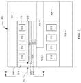
- FIG. 3 is a cross sectional view of a magnetic head, taken from line 3 - 3 of FIG. 2 and rotated 90 degrees counterclockwise, of a magnetic write head according to an embodiment of the present invention
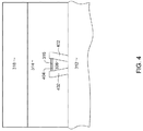
- FIG. 4 is an ABS view of a portion of the write head of FIG. 3 ;
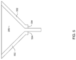
- FIG. 5 is a top down view of a write pole of the write head of FIG. 3 ;
- FIGS. 6-19 are views of a write head in various intermediate stages of manufacture illustrating method for manufacturing a write head according to an embodiment of the invention.
- FIGS. 20-35 are views of a write head in various intermediate stages of manufacture illustrating a method of manufacturing a write head according to an alternate embodiment of the invention.
- FIG. 1 there is shown a disk drive 100 embodying this invention.
- at least one rotatable magnetic disk 112 is supported on a spindle 114 and rotated by a disk drive motor 118 .
- the magnetic recording on each disk is in the form of annular patterns of concentric data tracks (not shown) on the magnetic disk 112 .
- At least one slider 113 is positioned near the magnetic disk 112 , each slider 113 supporting one or more magnetic head assemblies 121 . As the magnetic disk rotates, slider 113 moves radially in and out over the disk surface 122 so that the magnetic head assembly 121 may access different tracks of the magnetic disk where desired data are written.
- Each slider 113 is attached to an actuator arm 119 by way of a suspension 115 .
- the suspension 115 provides a slight spring force which biases slider 113 against the disk surface 122 .
- Each actuator arm 119 is attached to an actuator means 127 .
- the actuator means 127 as shown in FIG. 1 may be a voice coil motor (VCM).
- the VCM comprises a coil movable within a fixed magnetic field, the direction and speed of the coil movements being controlled by the motor current signals supplied by controller 129 .
- the rotation of the magnetic disk 112 generates an air bearing between the slider 113 and the disk surface 122 which exerts an upward force or lift on the slider.
- the air bearing thus counter-balances the slight spring force of suspension 115 and supports slider 113 off and slightly above the disk surface by a small, substantially constant spacing during normal operation.
- control unit 129 The various components of the disk storage system are controlled in operation by control signals generated by control unit 129 , such as access control signals and internal clock signals.
- control unit 129 comprises logic control circuits, storage means and a microprocessor.
- the control unit 129 generates control signals to control various system operations such as drive motor control signals on line 123 and head position and seek control signals on line 128 .
- the control signals on line 128 provide the desired current profiles to optimally move and position slider 113 to the desired data track on disk 112 .
- Write and read signals are communicated to and from write and read heads 121 by way of recording channel 125 .
- FIG. 2 is an ABS view of the slider 113 , and as can be seen the magnetic head including an inductive write head and a read sensor, is located at a trailing edge of the slider.
- the magnetic head including an inductive write head and a read sensor is located at a trailing edge of the slider.
- FIG. 1 The above description of a typical magnetic disk storage system, and the accompanying illustration of FIG. 1 are for representation purposes only. It should be apparent that disk storage systems may contain a large number of disks and actuators, and each actuator may support a number of sliders.
- the invention can be embodied in a magnetic head 300 .
- the write head includes a magnetic return pole 302 , and a magnetic back gap layer 304 connected with the return pole 302 in a region removed from the air bearing surface (ABS).
- a magnetic shaping layer 306 can be connected with the magnetic back gap layer 304
- a magnetic write pole 308 is connected with the shaping layer 306 such that the write pole 308 , shaping layer 306 , back gap 304 and return pole 302 are all magnetically connected with one another.
- the write pole 308 has a pole tip that extends to the ABS for emitting a magnetic write field toward a magnetic medium (not shown in FIG. 3 ).
- An electrically conductive write coil 310 passes through the write head structure 300 , and is embedded in one or more insulation layers 312 .
- the write coil 312 can be configured as one or more pancake coils or can be a helical coil having coil leads that pass above and below the write pole 312 (as shown in FIG. 3 ).
- the write head 300 can include a trailing magnetic shield 314 , located at the ABS, that is separated from the write pole by a trailing gap layer 316 .
- the trailing magnetic shield 314 can be connected with an upper (or trailing) return pole 318 that can magnetically connect the trailing magnetic shield 314 with the shaping layer 306 , back gap 304 and return pole 302 in a region removed from the ABS.
- the trailing magnetic shield increases writing speed by increasing the field gradient of the write field. To achieve this end, the thickness of the trailing gap 316 must be well controlled. If the trailing gap 316 is too large, the write field will not be increased and write speed will suffer. If the trailing gap is too small, too much flux will leak to the trailing shield 314 and the strength of the write field will suffer.
- the head 300 has a magnetic layer 320 formed over a portion of the write pole 308 , and a non-magnetic spacer layer 322 can be formed over the magnetic layer 320 .
- the layers 320 and 322 have a common front edge 324 located a desired distance from the ABS.
- the trailing magnetic shield 314 has a throat height TH that is the distance from the ABS to a back edge 326 of the trailing shield 314 .
- the write pole 308 has a flare point (not shown in FIG. 3 ) that is located at the location of the front edge 324 of the layers 320 , 322 .
- the location of the back edge 326 of the trailing shield is determined by the location of the front edge 324 of layers 320 , 322 and also by the thickness of the trailing gap layer 316 . This advantageously allows the throat height TH of the trailing shield 314 to be located relative to the flare point of the write pole 308 .
- the write pole has a trapezoidal shape at the ABS.
- the trailing shield 314 wraps around the sides of the write pole 308 , the trailing magnetic shield being separated from the sides of the write pole by first and second non-magnetic side gap layers 402 .
- the side gap layers preferably extend upward beyond the leading edge 404 of the write pole and even beyond the trailing gap layer 316 .
- FIG. 5 shows a top down view of the write pole 308 .
- the write pole 308 has outward extending stepped portions 502 that define a secondary flare point that can easily be located relative to the ABS.
- the outward extending stepped portions 502 each have a front edge 504 that defines the location of the flare point, and this location is self aligned with the front edge 324 of layers 320 , 322 described above with reference to FIG. 3 .
- the reason for this self alignment and the specific configuration of the outward extending stepped portions 502 will become clearer after reading the descriptions below of methods for manufacturing a write head according to an embodiment of the invention.
- a substrate 602 is provided.
- the substrate 602 can include, for example, the insulation layer 312 and all or a portion of the shaping layer 306 described above with reference to FIG. 3 .
- a layer of magnetic write pole material 604 is deposited full film over the substrate.
- the magnetic write pole material is preferably a lamination of magnetic layers separated by thin layers of non-magnetic material, and will be referred to herein as a laminate 604 .
- the write pole material 604 could be constructed as one or more layers of magnetic material without any lamination of non-magnetic layers.
- a magnetic layer 606 such as a layer of CoFe is deposited over the laminate 604 , and a non-magnetic spacer layer 608 is deposited over the magnetic layer 608 .
- the magnetic layer 606 can be deposited to a thickness of about 30-70 nm, and the non-magnetic spacer layer 608 can be deposited to a thickness of about 40-80 nm.
- the non-magnetic spacer layer 608 is preferably constructed of a material such as SiO 2 or SiN.
- An image transfer layer 610 is then, deposited over the spacer layer 608 .
- the image transfer layer 610 can be constructed of a polyimide material such as DURAMIDE®, or some similar material.
- a mask layer 612 is then formed over the layers 602 - 610 .
- the mask 612 can be formed by depositing a photoresist and then photolithographically patterning and developing the photoresist.
- the mask 612 has a front edge 614 that is located a desired distance from an intended air bearing surface plane, denoted by dashed line ABS in FIG. 6 .
- one or more reactive ion etching processes are performed to remove portions of the image transfer layer 610 and spacer layer 608 that are not protected by the mask 612 .
- the RIE is stopped when the magnetic layer 606 is reached.
- an ion milling is performed to remove portions of the magnetic layer 606 that are not protected by the layers 608 , 610 , 612 .
- Ion milling is terminated when the laminate layer 604 is reached.
- An end point detection method such as Secondary Ion Mass Spectroscopy (SIMS) can be used to determine when the laminate 604 has been reached.
- SIMS Secondary Ion Mass Spectroscopy
- a thin end point detection layer could be included at the top of the laminate 604 in order to assist SIMS end point detection.
- the remaining image transfer layer 610 and any remaining mask layer 612 FIG. 7 ), if any remains, can be lifted off.
- a hard mask layer 902 can be deposited over the laminate and over the magnetic layer 606 and spacer layer 608 .
- the hard mask layer 902 is preferably a laminate structure that includes a first layer 904 , a second layer 906 deposited over the first layer 904 and a third layer 908 deposited over the second layer 906 .
- the first layer is preferably alumina (Al 2 O 3 ) deposited to a thickness of 15-25 nm or about 20 nm.
- the second layer 906 is preferably a material that can be easily removed by reactive ion etch (RIE).
- the second layer 906 can be a material such as SiN or SiO 2 and can be deposited to a thickness of 25-35 nm or about 30 nm.
- the third layer is preferably a material that can be detected by an end point detection method such as Secondary Ion Mass Spectroscopy (SIMS).
- Layer 908 can be AlTiO deposited to a thickness of 15-25 nm or about 20 nm.
- the layers 904 , 906 , 908 can be deposited by a deposition method such as putter deposition that deposits the horizontally disposed surfaces at a rate about 3 times the rate at which vertically disposed surfaces are deposited.
- the total thickness of the hard mask layer 902 can have a thickness of about 55-85 nm or about 70 nm, having a vertically extending portion 910 (at the front edge of the layers 606 , 608 ) that has a thickness about 1 ⁇ 3 the thickness of the rest of the hard mask layer 602 .
- the vertical portion 910 of the hard mask layer 902 can have a thickness of about 18 to 28 nm or about 23 nm.
- an image transfer layer 1002 is deposited followed by a photoresist layer 1004 .
- the image transfer layer 1002 can be a polyimide material such as DURMIDE® and can be deposited to a thickness of about 1.2 um.
- the photoresist is photolithographically patterned to have a shape configured to define a write pole.
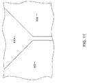
- An image transfer process such as Reactive Ion Etching (RIE) can then be performed to transfer the image of the photoresist layer 1004 onto the underlying image transfer layer 1002 ( FIG. 10 ). As seen in FIG. 11 , this reveals the hard mask 902 thereunder.
- RIE Reactive Ion Etching
- FIG. 12 a Reactive Ion Milling (RIM) is performed to remove portions of the hard mask layer 902 ( FIG. 10 ) that are not protected by the mask 1004 and image transfer layer 1002 .
- RIM Reactive Ion Milling
- FIG. 12 this reveals the non-magnetic spacer 608 and the laminate 604 .
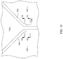
- FIGS. 13-15 an ion milling is performed to remove portions of the laminate 604 that are not protected by the mask structure 1004 .
- FIG. 14 shows a cross section as viewed from line 14 - 14 of FIG. 13 . As can be seen in FIG.
- the portions of the laminate 604 that are under the magnetic layer 606 and non-magnetic spacer layer 608 are under-milled, having an outward sloping base 1402 .
- This under-milling is due to shadowing from the extra height provided by the magnetic layer 606 and non-magnetic spacer 608 .
- FIG. 15 which is viewed from line 15 - 15 of FIG. 13
- the laminate tapers to form a trapezoidal shaped magnetic write pole tip. Therefore, the portion of the laminate 604 that is under the magnetic layer 606 and 608 extends outward to form a secondary flare point 1302 as can be seen with reference to FIG. 13 .
- the remaining image transfer layer 1002 can then be lifted off, such as by TMAH etch plus NMP and Reactive Ion Etch).
- a layer of non-magnetic material 1602 is conformally deposited.
- the layer 1602 is preferably alumina (Al 2 O 3 ) deposited by a method such as atomic layer deposition (ALD) or chemical vapor deposition (CVD).
- ALD atomic layer deposition
- CVD chemical vapor deposition
- another ion milling can be performed to preferentially remove horizontally disposed portions of the non-magnetic layer 1602 , resulting in non-magnetic sidewalls (side gap layers) 1602 being formed at either side of the write pole.
- This ion milling is preferably performed at an angle of about 55 degrees relative to normal.
- the hard mask layer 902 includes first, second and third layers 904 , 906 , 908 .
- the ion milling is performed sufficiently to remove the third layer 908 using Ti for endpoint detection, such as by SIMS.
- a reactive ion etching can be performed to remove the SiN second layer 906 leaving the first layer 904 as shown in FIG. 17 .
- the remaining hard mask layer 904 serves as a trailing gap layer, and the non-magnetic side walls 1602 serve as first and second non-magnetic side gaps.
- an electrically conductive (preferably magnetic) seed layer 1802 such as Rh is deposited full film.
- a masking and electroplating process can be performed to deposit a magnetic material to form a trailing magnetic shield 1902 .
- the trailing, wrap around, magnetic shield 1902 has a throat height TH measured from an intended ABS plane that is defined by the location of the front edge of the layers 606 , 608 and by the thickness of the hard mask layers 902 (including all three layers 904 , 906 , 908 ).
- TH measured from an intended ABS plane that is defined by the location of the front edge of the layers 606 , 608 and by the thickness of the hard mask layers 902 (including all three layers 904 , 906 , 908 ).
- the location of the secondary flare write head flare point 1302 is aligned with the front edge of the layers 606 , 608 . Therefore, the spacing between the trailing shield 1902 ( FIG. 19 ) and the flare point 1302 is determined by the thickness of the layers 902 (including layers 904 , 906 and 908 .
- the ABS will be defined by a lapping operation that removes material from the left side of the page as shown in FIG. 19 , stopping the lapping at the intended ABS plane indicated by the dashed line denoted “ABS”.
- FIGS. 20-35 another method for constructing a magnetic write head according to an embodiment of the invention is disclosed.
- a substrate 2002 is provided.
- a laminate 2004 is deposited over the substrate.
- a magnetic layer such as CoFe 2006 having a thickness of 30-70 nm or about 50 nm is deposited over the laminate 2004 .
- a non-magnetic layer 2008 (preferably Rh Ir or Ru) is deposited over the magnetic layer 2006 .
- the non-magnetic layer can have a thickness of 40-80 nm or about 60 nm.
- An image transfer layer 2010 constructed of a polyimide material such as DURMIDE® is deposited over the non-magnetic spacer layer 2008 , and a layer of photoresist 2012 is deposited over the image transfer layer 2010 .
- FIG. 21 which shows a top down view as viewed from the line 21 - 21 of FIG. 20
- the photoresist 2012 is photolithographically patterned and the image of the photoresist layer 2012 is transferred onto the underlying image transfer layer 2010 ( FIG. 20 ) to reveal a portion of the non-magnetic spacer layer 2008 .
- An ion milling is performed to remove portions of the magnetic layer 2006 and non-magnetic spacer layer 2008 that are not protected by the mask 2012 .
- the mask 2012 can then be lifted off, leaving a structure as shown in FIG. 22 .
- FIG. 22 shows a side, cross sectional view taken from the line 22 - 22 of FIG. 21 .
- a thin alumina mask layer 2302 is deposited full film to a thickness of 5-15 nm or about 10 nm.
- a layer of material that is resistant to chemical mechanical polishing (CMP stop layer) 2304 is deposited over the thin alumina mask 2302 .
- the CMP stop layer 2304 can be a material such as diamond like carbon (DLC) and can be deposited to a thickness of 15-25 nm or about 20 nm.
- An image transfer layer such as DURAMIDE® 2306 is deposited relatively thick (such as to a thickness of about 1000-1400 nm or about 1200 nm.
- a layer of photoresist 2308 is deposited over the image transfer layer 2306 .
- the photoresist layer 2308 is photolithographically patterned to define a write pole, and the image of the photoresist layer 2308 is transferred onto the underlying image transfer layer 2306 .
- a reactive ion etch is performed to remove portions of the CMP stop layer 2304 that are not protected by the mask.
- the resulting structure can be seen with reference to FIG. 24 , which shows a top down view as viewed from line 24 - 24 of FIG. 23 .
- an ion milling is performed to remove portions of the laminate layer that are not protected by the mask structure. The ion milling removes the photoresist layer leaving the image transfer layer 2306 as a mask.
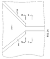
- the wide stepped flare 2004 2602 forms a secondary flare point having a front edge 2502 as seen in FIG. 25 .
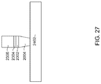
- a layer of non-magnetic side gap material 2802 is deposited.
- the layer 2802 is preferably alumina, deposited by a conformal deposition method such as ALD or CVD, and can be deposited to a thickness of 45-55 nm or about 50 nm.
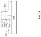
- a time-controlled ion milling is performed to recess the alumina layer 2802 and to define side walls having a desired thickness as shown in FIG. 29 .
- the resulting non-magnetic side walls 802 can have a thickness of, for example, 65-75 nm or about 70 nm.
- a refill layer 3002 is deposited.
- the refill layer can be, for example SiO 2 .
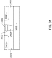
- a chemical mechanical polishing process (CMP) is performed.
- the CMP process removes the remaining image transfer layer 2306 and forms a planar surface, as shown in FIG. 31 .
- FIG. 33 shows a side, cross sectional view of the structure thus far, the view being taken from line 33 - 33 of FIG. 32 .
- the thin alumina mask 2302 extends over the magnetic layer 2006 and non-magnetic spacer layer 2008 .
- a Ru seed 3402 layer having a thickness of 20-30 nm or about 25 nm is deposited, followed by a CoFe seed layer 3404 that can be thinner, such as about 5 nm thick.
- a masking and plating operation can be performed to deposit a magnetic material to form a magnetic trailing shield 3502 .
- the Ru layer 3402 and thin alumina layer 2302 together define the thickness of a trailing gap for the magnetic shield 3502 .
Landscapes
- Engineering & Computer Science (AREA)
- Manufacturing & Machinery (AREA)
- Physics & Mathematics (AREA)
- Electromagnetism (AREA)
- Magnetic Heads (AREA)
Abstract
Description
Claims (20)
Priority Applications (1)
| Application Number | Priority Date | Filing Date | Title |
|---|---|---|---|
| US11/956,277 US7881010B2 (en) | 2007-12-13 | 2007-12-13 | Process for self-aligned flare point and shield throat definition prior to main pole patterning |
Applications Claiming Priority (1)
| Application Number | Priority Date | Filing Date | Title |
|---|---|---|---|
| US11/956,277 US7881010B2 (en) | 2007-12-13 | 2007-12-13 | Process for self-aligned flare point and shield throat definition prior to main pole patterning |
Publications (2)
| Publication Number | Publication Date |
|---|---|
| US20090152234A1 US20090152234A1 (en) | 2009-06-18 |
| US7881010B2 true US7881010B2 (en) | 2011-02-01 |
Family
ID=40751834
Family Applications (1)
| Application Number | Title | Priority Date | Filing Date |
|---|---|---|---|
| US11/956,277 Expired - Fee Related US7881010B2 (en) | 2007-12-13 | 2007-12-13 | Process for self-aligned flare point and shield throat definition prior to main pole patterning |
Country Status (1)
| Country | Link |
|---|---|
| US (1) | US7881010B2 (en) |
Cited By (2)
| Publication number | Priority date | Publication date | Assignee | Title |
|---|---|---|---|---|
| US20090110960A1 (en) * | 2007-10-25 | 2009-04-30 | Tdk Corporation | Method of etching magnetoresistive film by using a plurality of metal hard masks |
| US20090168258A1 (en) * | 2007-12-28 | 2009-07-02 | Quang Le | Hybrid, self aligned magnetic write head with a partially plated pole and method of producing same |
Families Citing this family (4)
| Publication number | Priority date | Publication date | Assignee | Title |
|---|---|---|---|---|
| US8068312B2 (en) * | 2007-11-21 | 2011-11-29 | Hitachi Global Technologies Netherlands B.V. | Perpendicular magnetic write head with stitched notched trailing shield |
| US7990651B2 (en) * | 2007-12-13 | 2011-08-02 | Hitachi Global Storage Technologies Netherlands B.V. | Method of manufacturing a perpendicular magnetic write head with stepped trailing magnetic shield with electrical lapping guide control |
| US20120231296A1 (en) * | 2011-03-11 | 2012-09-13 | Hitachi Global Storage Technologies Netherlands B.V. | Method for manufacturing an advanced magnetic read sensor |
| FR3009130B1 (en) * | 2013-07-26 | 2016-11-18 | Commissariat Energie Atomique | METHOD FOR MANUFACTURING A SPACER FOR A DOUBLE-SCALE ELECTRONIC MEMORY CELL AND A MEMORY ELECTRONIC MEMORY CELL |
Citations (20)
| Publication number | Priority date | Publication date | Assignee | Title |
|---|---|---|---|---|
| US5935644A (en) | 1996-11-15 | 1999-08-10 | International Business Machines Corporation | Method of making thin film induction recording head having an inset first insulation layer that defines zero throat height and pole tip apex angle |
| US20020026705A1 (en) | 1998-08-12 | 2002-03-07 | Santini Hugo Alberto Emilio | Method of making a write head with multi-stitched second pole piece |
| US6477765B1 (en) * | 1999-11-04 | 2002-11-12 | Storage Technology Corporation | Method of fabricating a magnetic write transducer |
| US6553649B1 (en) | 1998-04-10 | 2003-04-29 | Hitachi Global Storage Technologies Netherlands Bv | Method of making a write head before read head constructed merged magnetic head with track width and zero throat height defined by first pole tip |
| US6557242B1 (en) | 1998-04-10 | 2003-05-06 | International Business Machines Corporation | Method of making a write head with self-aligned pedestal shaped pole tips that are separated by a zero throat height defining layer |
| US6560853B1 (en) | 1998-04-10 | 2003-05-13 | International Business Machines Corporation | Method of making inductive head with reduced height insulation stack due to partial coverage zero throat height defining insulation layer |
| US20030137779A1 (en) | 2002-01-18 | 2003-07-24 | International Business Machines Corporation | Perpendicular recording write head with a ferromagnetic shaping layer |
| US20050068669A1 (en) | 2003-09-26 | 2005-03-31 | Yimin Hsu | Head for perpendicular recording with a floating trailing shield |
| US20060002024A1 (en) | 2004-06-30 | 2006-01-05 | Quang Le | Method and apparatus for defining leading edge taper of a write pole tip |
| US20060002016A1 (en) | 2004-06-30 | 2006-01-05 | Vladimir Nikitin | Method and apparatus for processing sub-micron write head flare definition |
| US20060012914A1 (en) | 2004-07-13 | 2006-01-19 | Sae Magnetics (H.K.) Ltd. | Thin film magnetic head, head gimbals assembly, head arm assembly, magnetic recording apparatus, and method of manufacturing thin film magnetic head |
| US20060044682A1 (en) | 2004-08-31 | 2006-03-02 | Quang Le | Self aligned wrap around shield for perpendicular magnetic recording |
| US7061717B2 (en) | 2003-05-22 | 2006-06-13 | Headway Technologies, Inc. | Yoke structure with constricted width |
| US7061719B2 (en) | 2002-10-01 | 2006-06-13 | Tdk Corporation | Thin film magnetic head and method of manufacturing the same |
| US20060238916A1 (en) | 2005-04-20 | 2006-10-26 | Headway Technologies, Inc. | Thin film magnetic head and manufacturing method thereof |
| US7151647B2 (en) | 2003-10-10 | 2006-12-19 | Headway Technologies, Inc. | Thin film magnetic head and manufacturing method for creating high surface recording density and including a second yoke portion having two layers of which one is etched to form a narrow portion and a sloped flare portion |
| US7159302B2 (en) | 2004-03-31 | 2007-01-09 | Hitachi Global Storage Technologies Netherlands B.V. | Method for manufacturing a perpendicular write head |
| US20080074782A1 (en) * | 2006-09-21 | 2008-03-27 | Hitachi Global Storage Technologies | Magnetic write head having a stair notched, steep shouldered pole and a write gap bump |
| US7587811B2 (en) * | 2006-04-25 | 2009-09-15 | Hitachi Global Storage Technologies Netherlands B.V. | Method for manufacturing a magnetic write head for perpendicular magnetic data recording |
| US7715147B2 (en) * | 2006-10-27 | 2010-05-11 | Hitachi Global Storage Technologies Netherlands B.V. | Magnetic write head having a shield that extends below the leading edge of the write pole |
-
2007
- 2007-12-13 US US11/956,277 patent/US7881010B2/en not_active Expired - Fee Related
Patent Citations (21)
| Publication number | Priority date | Publication date | Assignee | Title |
|---|---|---|---|---|
| US5935644A (en) | 1996-11-15 | 1999-08-10 | International Business Machines Corporation | Method of making thin film induction recording head having an inset first insulation layer that defines zero throat height and pole tip apex angle |
| US20030137771A1 (en) | 1998-04-10 | 2003-07-24 | Emilio Santini Hugo Alberto | Method of making a write head with self-aligned pedestal shaped pole tips which are separated by a zero throat height defining layer |
| US6553649B1 (en) | 1998-04-10 | 2003-04-29 | Hitachi Global Storage Technologies Netherlands Bv | Method of making a write head before read head constructed merged magnetic head with track width and zero throat height defined by first pole tip |
| US6557242B1 (en) | 1998-04-10 | 2003-05-06 | International Business Machines Corporation | Method of making a write head with self-aligned pedestal shaped pole tips that are separated by a zero throat height defining layer |
| US6560853B1 (en) | 1998-04-10 | 2003-05-13 | International Business Machines Corporation | Method of making inductive head with reduced height insulation stack due to partial coverage zero throat height defining insulation layer |
| US20020026705A1 (en) | 1998-08-12 | 2002-03-07 | Santini Hugo Alberto Emilio | Method of making a write head with multi-stitched second pole piece |
| US6477765B1 (en) * | 1999-11-04 | 2002-11-12 | Storage Technology Corporation | Method of fabricating a magnetic write transducer |
| US20030137779A1 (en) | 2002-01-18 | 2003-07-24 | International Business Machines Corporation | Perpendicular recording write head with a ferromagnetic shaping layer |
| US7061719B2 (en) | 2002-10-01 | 2006-06-13 | Tdk Corporation | Thin film magnetic head and method of manufacturing the same |
| US7061717B2 (en) | 2003-05-22 | 2006-06-13 | Headway Technologies, Inc. | Yoke structure with constricted width |
| US20050068669A1 (en) | 2003-09-26 | 2005-03-31 | Yimin Hsu | Head for perpendicular recording with a floating trailing shield |
| US7151647B2 (en) | 2003-10-10 | 2006-12-19 | Headway Technologies, Inc. | Thin film magnetic head and manufacturing method for creating high surface recording density and including a second yoke portion having two layers of which one is etched to form a narrow portion and a sloped flare portion |
| US7159302B2 (en) | 2004-03-31 | 2007-01-09 | Hitachi Global Storage Technologies Netherlands B.V. | Method for manufacturing a perpendicular write head |
| US20060002016A1 (en) | 2004-06-30 | 2006-01-05 | Vladimir Nikitin | Method and apparatus for processing sub-micron write head flare definition |
| US20060002024A1 (en) | 2004-06-30 | 2006-01-05 | Quang Le | Method and apparatus for defining leading edge taper of a write pole tip |
| US20060012914A1 (en) | 2004-07-13 | 2006-01-19 | Sae Magnetics (H.K.) Ltd. | Thin film magnetic head, head gimbals assembly, head arm assembly, magnetic recording apparatus, and method of manufacturing thin film magnetic head |
| US20060044682A1 (en) | 2004-08-31 | 2006-03-02 | Quang Le | Self aligned wrap around shield for perpendicular magnetic recording |
| US20060238916A1 (en) | 2005-04-20 | 2006-10-26 | Headway Technologies, Inc. | Thin film magnetic head and manufacturing method thereof |
| US7587811B2 (en) * | 2006-04-25 | 2009-09-15 | Hitachi Global Storage Technologies Netherlands B.V. | Method for manufacturing a magnetic write head for perpendicular magnetic data recording |
| US20080074782A1 (en) * | 2006-09-21 | 2008-03-27 | Hitachi Global Storage Technologies | Magnetic write head having a stair notched, steep shouldered pole and a write gap bump |
| US7715147B2 (en) * | 2006-10-27 | 2010-05-11 | Hitachi Global Storage Technologies Netherlands B.V. | Magnetic write head having a shield that extends below the leading edge of the write pole |
Non-Patent Citations (2)
| Title |
|---|
| Batra et al., "A Perpendicular Write Head Design for High Density Recording" IEEE Transactions on Magnetics, vol. 38, No. 1, Jan. 2002. |
| Williams et al., "Perpendicular Write Process and Head Design" IEEE Transactions on Magnetics, vol. 38, No. 4, Jul. 2002. |
Cited By (4)
| Publication number | Priority date | Publication date | Assignee | Title |
|---|---|---|---|---|
| US20090110960A1 (en) * | 2007-10-25 | 2009-04-30 | Tdk Corporation | Method of etching magnetoresistive film by using a plurality of metal hard masks |
| US8298430B2 (en) * | 2007-10-25 | 2012-10-30 | Tdk Corporation | Method of etching magnetoresistive film by using a plurality of metal hard masks |
| US20090168258A1 (en) * | 2007-12-28 | 2009-07-02 | Quang Le | Hybrid, self aligned magnetic write head with a partially plated pole and method of producing same |
| US8031434B2 (en) * | 2007-12-28 | 2011-10-04 | Hitachi Global Storage Technologies Netherlands B.V. | Hybrid, self aligned magnetic write head with a partially plated pole and method of producing same |
Also Published As
| Publication number | Publication date |
|---|---|
| US20090152234A1 (en) | 2009-06-18 |
Similar Documents
| Publication | Publication Date | Title |
|---|---|---|
| US8323727B2 (en) | Method for manufacturing a perpendicular magnetic write head having a tapered write pole and a stepped wrap around side shield gap | |
| US8000059B2 (en) | Perpendicular magnetic write head with a thin wrap around magnetic shield | |
| US7576951B2 (en) | Perpendicular magnetic write head having a magnetic write pole with a concave trailing edge | |
| US8201320B2 (en) | Method for manufacturing a magnetic write head having a wrap around shield that is magnetically coupled with a leading magnetic shield | |
| US8347488B2 (en) | Magnetic write head manufactured by damascene process producing a tapered write pole with a non-magnetic step and non-magnetic bump | |
| US7963024B2 (en) | Method of manufacturing a magnetic write head for perpendicular magnetic recording | |
| US8110085B2 (en) | Assisted deposition, narrow trench damascene process for manufacturing a write pole of a magnetic write head | |
| US8441757B2 (en) | Perpendicular magnetic write head with wrap-around shield, slanted pole and slanted pole bump fabricated by damascene process | |
| US8339734B2 (en) | Magnetic write head having a wrap around trailing shield with an asymetrical side gap | |
| US7990651B2 (en) | Method of manufacturing a perpendicular magnetic write head with stepped trailing magnetic shield with electrical lapping guide control | |
| US7506431B2 (en) | Method of manufacturing a perpendicular magnetic write head having a wrap-around trailing shield and a concave trailing edge main pole | |
| US8451562B2 (en) | Method for manufacturing a magnetic write head having a wrap around trailing magnetic shield with a tapered side gap | |
| US20090144966A1 (en) | Leading edge tapered bump with electrical lapping guide control for wrap around shield | |
| US8503131B2 (en) | Perpendicular magnetic write head having a novel shield structure | |
| US20100157472A1 (en) | Magnetic write head having a self-aligned side wrap-around shield with multi-angle slanted bump | |
| US8137570B2 (en) | Additive write pole process for wrap around shield | |
| US7788798B2 (en) | Method for manufacturing a perpendicular magnetic write head with wrap around magnetic trailing and side shields | |
| US7881010B2 (en) | Process for self-aligned flare point and shield throat definition prior to main pole patterning | |
| US8568601B2 (en) | Fenceless main pole definition for advanced perpendicular magnetic write head | |
| US20100155364A1 (en) | Magnetic write head having a stepped trailing shield and write pole with a sloped trailing edge | |
| US8349197B2 (en) | Method for manufacturing a perpendicular magnetic write head having a tapered write pole and non-magnetic bump structure | |
| US8252190B2 (en) | Method for manufacturing a magnetic write head having a hard mask defined write pole trailing edge step | |
| US8318031B2 (en) | Method for manufacturing a perpendicular magnetic write head having a tapered write pole | |
| US8136228B2 (en) | Method for manufacturing a magnetic write head | |
| US20100155232A1 (en) | Method for manufacturing a magnetic write head having a write pole trailing edge taper |
Legal Events
| Date | Code | Title | Description |
|---|---|---|---|
| AS | Assignment |
Owner name: HITACHI GLOBAL STORAGE TECHNOLOGIES NETHERLANDS B. Free format text: ASSIGNMENT OF ASSIGNORS INTEREST;ASSIGNORS:GUTHRIE, HUNG-CHIN;JIANG, MING;LEE, EDWARD HIN PONG;AND OTHERS;REEL/FRAME:020791/0805;SIGNING DATES FROM 20071211 TO 20071212 Owner name: HITACHI GLOBAL STORAGE TECHNOLOGIES NETHERLANDS B. Free format text: ASSIGNMENT OF ASSIGNORS INTEREST;ASSIGNORS:GUTHRIE, HUNG-CHIN;JIANG, MING;LEE, EDWARD HIN PONG;AND OTHERS;SIGNING DATES FROM 20071211 TO 20071212;REEL/FRAME:020791/0805 |
|
| FEPP | Fee payment procedure |
Free format text: PAYOR NUMBER ASSIGNED (ORIGINAL EVENT CODE: ASPN); ENTITY STATUS OF PATENT OWNER: LARGE ENTITY |
|
| STCF | Information on status: patent grant |
Free format text: PATENTED CASE |
|
| AS | Assignment |
Owner name: HGST, NETHERLANDS B.V., NETHERLANDS Free format text: CHANGE OF NAME;ASSIGNOR:HGST, NETHERLANDS B.V.;REEL/FRAME:029341/0777 Effective date: 20120723 Owner name: HGST NETHERLANDS B.V., NETHERLANDS Free format text: CHANGE OF NAME;ASSIGNOR:HITACHI GLOBAL STORAGE TECHNOLOGIES NETHERLANDS B.V.;REEL/FRAME:029341/0777 Effective date: 20120723 |
|
| FPAY | Fee payment |
Year of fee payment: 4 |
|
| AS | Assignment |
Owner name: WESTERN DIGITAL TECHNOLOGIES, INC., CALIFORNIA Free format text: ASSIGNMENT OF ASSIGNORS INTEREST;ASSIGNOR:HGST NETHERLANDS B.V.;REEL/FRAME:040826/0821 Effective date: 20160831 |
|
| MAFP | Maintenance fee payment |
Free format text: PAYMENT OF MAINTENANCE FEE, 8TH YEAR, LARGE ENTITY (ORIGINAL EVENT CODE: M1552) Year of fee payment: 8 |
|
| AS | Assignment |
Owner name: JPMORGAN CHASE BANK, N.A., AS AGENT, ILLINOIS Free format text: SECURITY INTEREST;ASSIGNOR:WESTERN DIGITAL TECHNOLOGIES, INC.;REEL/FRAME:052915/0566 Effective date: 20200113 |
|
| AS | Assignment |
Owner name: WESTERN DIGITAL TECHNOLOGIES, INC., CALIFORNIA Free format text: RELEASE OF SECURITY INTEREST AT REEL 052915 FRAME 0566;ASSIGNOR:JPMORGAN CHASE BANK, N.A.;REEL/FRAME:059127/0001 Effective date: 20220203 |
|
| FEPP | Fee payment procedure |
Free format text: MAINTENANCE FEE REMINDER MAILED (ORIGINAL EVENT CODE: REM.); ENTITY STATUS OF PATENT OWNER: LARGE ENTITY |
|
| LAPS | Lapse for failure to pay maintenance fees |
Free format text: PATENT EXPIRED FOR FAILURE TO PAY MAINTENANCE FEES (ORIGINAL EVENT CODE: EXP.); ENTITY STATUS OF PATENT OWNER: LARGE ENTITY |
|
| STCH | Information on status: patent discontinuation |
Free format text: PATENT EXPIRED DUE TO NONPAYMENT OF MAINTENANCE FEES UNDER 37 CFR 1.362 |
|
| FP | Lapsed due to failure to pay maintenance fee |
Effective date: 20230201 |


