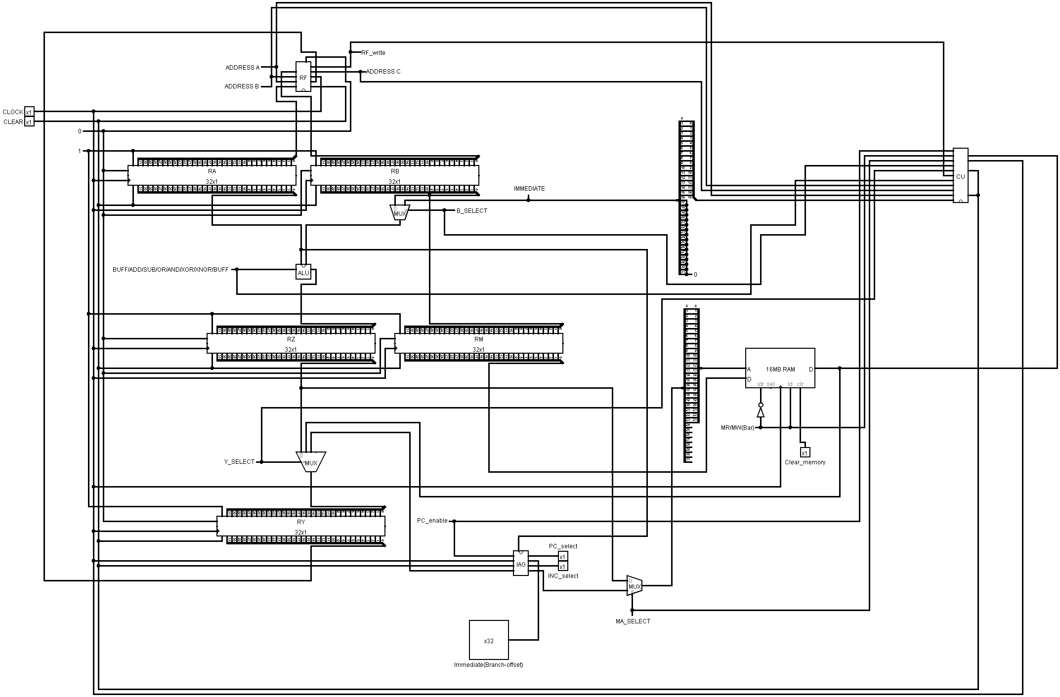
Data path in a processor refers to flow of data during execution of any instruction from instruction register given in definite format. For eg. If instruction is add,r1,r2,r3 i.e add the content of registers r1 and r2 then put the result in register r1 then in order to execute that instruction, processor has to go through different stages which is given by data path in that processor.
There are 32 general purpose registers(GPR) which can be used at any stage and time. All 32 general purpose registers along with few more circuitry constitute register file of data path. Second important unit used is Arithmetic logic Unit(ALU) which is ,in my circuit, capable of performing addition, subtraction, and, or, xor and xnor operations. ALU is also capable of transferring the date without changing anything which is required in “mov” operation. The result of ALU is stored in the register RZ. Now, if any memory operation is involved then it is performed in this step. In last step if data has to be stored in a GPR then it is written back to GPR. CU signals are generated on the basis of opcode and content of IR. Each instruction takes five clock cycles to get executed.
The circuit made is capable of handling 8 instructions – “add”, “adi”, “mov”, “lda”, “sta”, “sub”, “and”, “mvi” where each instruction has different meaning and task. Syntax and resiter transfer notation of each instruction are as follows:
| Opcode | Binary Equivalent | Syntax | Register Transfer Notation |
|---|---|---|---|
| add | 000000 | add ri,rj,rk | ri<-[rj]+[rk] |
| adi | 100000 | adi ri,rj,XXXX | ri<-[rj]+XXXX |
| mov | 001000 | mov ri,rj | ri<-[rj] |
| lda | 101000 | lda ri,XXXX(rj) | ri<-[[ri]+XXXX] |
| sta | 110000 | sta ri,XXXX(rj) | XXXX+[rj]<-[ri] |
| sub | 010000 | sub ri,rj,rk | ri<-rj-rk |
| and | 011000 | and ri,rj,rk | ri<-[rj]&[rk] |
| mvi | 111000 | mov ri,XXXX | ri<-XXXX |
31>=i,j,k>=0
XXXX is any four digit hexadecimal value.
The 32-instruction register has following way of storing instruction:
-
R-type
Opcode(6) Rd(5) Rs1(5) Rs2(5) Sh(5) Func(6) -
I type
Opcode(6) Rd(5) Rs1(5) Immediate(16)
Where Rd is destination register , Rs1,Rs2 are source registers, Sh and func are for special function(my circuits don’t use them)
- Address of each register is of 5 bit starting from 00000 to 11111.
Here, I assumed that the machine code of program is getting stored in the same main memory at address starting from (00000000)h(We assume that program counter is initially at 00000000h). So, first task is how to get machine code for your instructions. To accomplish this, run the Java program then enter the number of instruction you want to execute followed by that number of instructions. The output of program give you the machine code for your instructions. For eg. You want to execute the following instructions -
lda r1,0007(r2)
lda r2,0007(r3)
add r3,r1,r2
sta r3,0000(r3)
Then machine code generated will be –
a0220007
a0430007
00611000
c0630000
Next task is to store these machine code manually in main memory at consecutive location starting from (00000000)h. Then give clock. After every 5 clock cycles each instruction get executed and program counter will jump to next location. That’s it. “You’re done”. You can check the content of memory to check your outputs.
All the circuit in the complete_datapath.circ strictly follow the circuits given in the book “Computer Organization” by Carl Hamacher.
