This CPU design is based on Ben Eater's tutorial on building an 8-Bit breadboard computer. The CPU is implemented in an FPGA using VHDL and follows the same architecture as described in the tutorial.
This small project was done to get familiar with FPGAs, digital circuit design and how a CPU works. The CPU use both combinational (Does not require a clock) and sequential logic (Requires a clock). FPGA needs simulation to debug hardware problems and therefore testbenches are required. Testbenches for most of the modules are provided.
The FPGA used is an Altera Cyclone IV EP4CE6E22C8N.
-
- 8-Bit ALU
- Carry Flag (CF) and Zero Flag (ZF) bits for the flags register
- 8-Bit ALU registers A and B (A is used as the accumulator)
- Instruction register (4-Bit opcode and 4-Bit operand)
- Instruction decoder with 16 control line outputs
- 4-Bit memory address register
- 16 Bytes of RAM
- 4-Bit program counter
- 8-Bit wide bus for both data and addressing (Multiplexed not bidirectional)
- Manually adjustable clocks with 4 levels (1Hz, 5Hz, 10Hz, 25Hz) derived from a 50 MHz clock
-
- 4 digit, 7-segment display for outputting the results (Multiplexed)
- 8-Bit binary to BCD converter for output to 7-segment display (Double dabble algorithm in VHDL)
- Debug LEDs to see what is happening in the registers (Multiplexed)
- Debounce for DIP switches and momentary push buttons (Switch Debounce Nandland Tutorial)
The following instruction set is currently implemented in the 8-Bit CPU. All the opcodes contains only one operand.
| Opcode | Opcode in binary | Operand | Description |
|---|---|---|---|
| NOP | 0000 | - | No operation |
| LDA | 0001 | Address of variable | Load register A |
| ADD | 0010 | Address of variable | Adds and puts the result in A register |
| SUB | 0011 | Address of variable | Subtracts and puts the result in A register |
| STA | 0100 | Address in RAM | Stores the value in A register to RAM |
| LDI | 0101 | Binary value | Loads a value immediately into A register |
| JMP | 0110 | Address to jump to | Unconditional jump |
| JC | 0111 | Address to jump to | Jump only if the carry flag is set |
| JZ | 1000 | Address to jump to | Jump only if the zero flag is set |
| OUT | 1110 | - | Output the result to the 7-segment display |
| HALT | 1111 | - | Stops the CPU clock |
The programs written for the CPU are stored in the RAM. Each instruction is fetched from the RAM and executed. To change the program check the single_port_ram.vhd file. Example for a simple add program is given below.
--Example for simple addition
signal r_ram : memory_t := (
                            "00011110", --LDA 14
                            "00101111",	--ADD 15
                            "11100000",	--OUT
                            "11110000", --HALT
                            "00000000",
                            "00000000",
                            "00000000",
                            "00000000",
                            "00000000",
                            "00000000",
                            "00000000",
                            "00000000",
                            "00000000",
                            "00000000",
                            "00111000", --56 in binary at address 14
                            "00011100"  --28 in binary at address 15
                           );
Manually writing to RAM using DIP switches is not implemented.
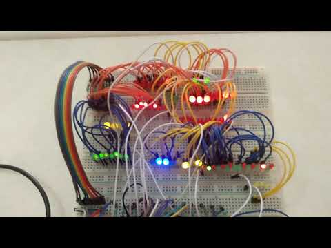
Video demonstration of the CPU in action.
The following simulation is for a simple add program that loads the values from ram and then stores the result of the addition in A register. The test_cpu.vhd testbench was used for the simulation.
