This code example demonstrates the Programmable Gain Amplifier (PGA) feature inside the Analog-to-Digital Converter (ADC) of the ATtiny1627 family of microcontrollers.
- MPLAB® X IDE v6.05 or newer
- MPLAB XC8 v2.41 or newer
- MPLAB Data Visualizer Plugin or alternative serial COM port terminal
- MPLAB Code Configurator (MCC) v5.0.2 or newer
- MPLAB Code Configurator (MCC) Device Libraries 8-bit AVR MCUs v2.7.0
- Microchip ATtiny_DFP (v2.5.116) or newer
Note: For all older DFPs, change line 60 in main.c from ADC0.MUXPOS |= (ADC_VIA_0_bm); to ADC0.MUXPOS |= (ADC_VIA0_bm);.
This demonstration only requires the ATtiny1627 Curiosity Nano connected to a PC via USB.
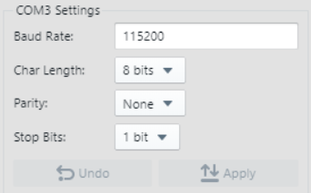
The baud rate for the board is 115200, no parity, and 1 stop bit.
Note: If MPLAB Data Visualizer is not installed, then the icon will not appear in the toolbar. (This example uses the plug-in version). MPLAB Data Visualizer can be downloaded from here.
To setup MPLAB Data Visualizer as a serial terminal:
- Plug in the ATtiny1627 Curiosity Nano.
- Click on the plugin icon in the MPLAB X IDE toolbar.
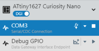
- Select the Curiosity Nano in the COM port list, but do not connect to it.
- In the lower left corner of the screen setup the baud rate and bit settings as shown.
- Press the play button next to the name to connect to the COM port.
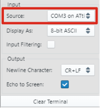
- In the terminal viewer, select the connected COM port in source options.
The ATtiny1627 contains a capacitive-based PGA that can be used to amplify small signals in order to improve signal resolution in the ADC. For this demonstration, the internal signal DAC (DACREF in the datasheet) is measured, with a set value of 100mV. However, using MPLAB Code Configurator (MCC), the positive input channel can be changed to an external pin, if desired. Any signal applied to this pin should not exceed the maximum ratings specified in the datasheet.
Note: If any changes are made in MCC, the configuration must be re-generated to change the API's behavior.
Figure 1 - Positive Input Multiplexer Setting
The voltage reference level used by the ADC can also be changed. Smaller voltage references have better measurement resolution, while larger references have a wider input span. A voltage reference larger than the supply voltage of the microcontroller cannot be used.
Note: The external VREF and VDD options produce a result relative to their value, e.g.: 20% (of VDD).
In this example, the PGA is used to multiply the input signal. The demo goes through all of the PGA settings: NO PGA, 1x, 2x, 4x, 8x, and 16x.
To trigger the ADC, the Event System was used to connect the Periodic Interrupt Timer (PIT) to the ADC Start Trigger. The PIT runs at 1kHz, but is divided by 2048 in the event channel. This creates a period of ~2 seconds between each conversion. LED0 on the Curiosity Nano is also connected to the same event channel. Visually, every time the LED on the Curiosity Nano goes from ON to OFF, the ADC is triggered.
For simplicity, the microcontroller remains in sleep most of the time. When the ADC completes the conversion, the interrupt generated wakes the microcontroller from sleep to process the result. After processing and printing the result, the ADC-PGA configuration is changed. Then, the microcontroller goes back to sleep to wait for the next cycle.
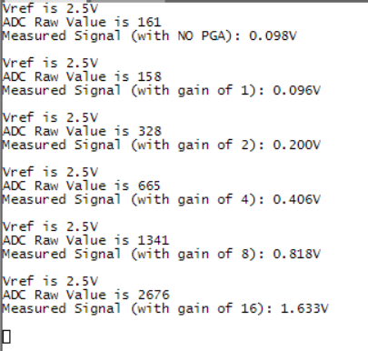
Figure 2 - Output from the Example. VREF = 2.5V, VDD = 5V
Note: VDD on the Curiosity Nano is 3.3V by default.
One downside of this approach is that the program is sensitive to interrupts. As an example, moving to interrupt driven UART would trigger the program to run early, causing the output to duplicate infinitely. One workaround would be to set (and clear) a software flag that is triggered from the ADC's interrupt.
In some versions of MCC, there are 2 warnings that are triggered:
- "ADC0: Enable Peripheral"
- "ADC0: Set MUXPOS and MUXNEG to 'Via PGA'"
These warnings can be ignored in this example.
The nominal voltage of DACREF is 100mV. In figure 2, the error of the measurement increases as the gain goes up. This is primarily from 2 sources - offset error and gain error.
-
Offset error is a static level shift that appears on the input. This offset is affected by the gain of the PGA.
-
Gain error is the deviation from the expected gain value, e.g.: the expected gain of 16x is actually 15.9x. As the gain increases, the accuracy of the gain goes down.
Curiosity Nano development boards ship running at 3.3V. To change the operating voltage to 5V (or another level), please consult section 3.3 in the ATtiny1627 Curiosity Nano User's Guide.
This code example demonstrates the Programmable Gain Amplifier in the ATtiny1627 family of microcontrollers.


