The code in this repository lets you control an SDRAM chip without licensing IP from anyone.
- Take files from
src/and add them to your own project. If you use hdlmake, you can add this repository itself as a remote module. - Other helpful modules are also available in this GitHub organization.
- See
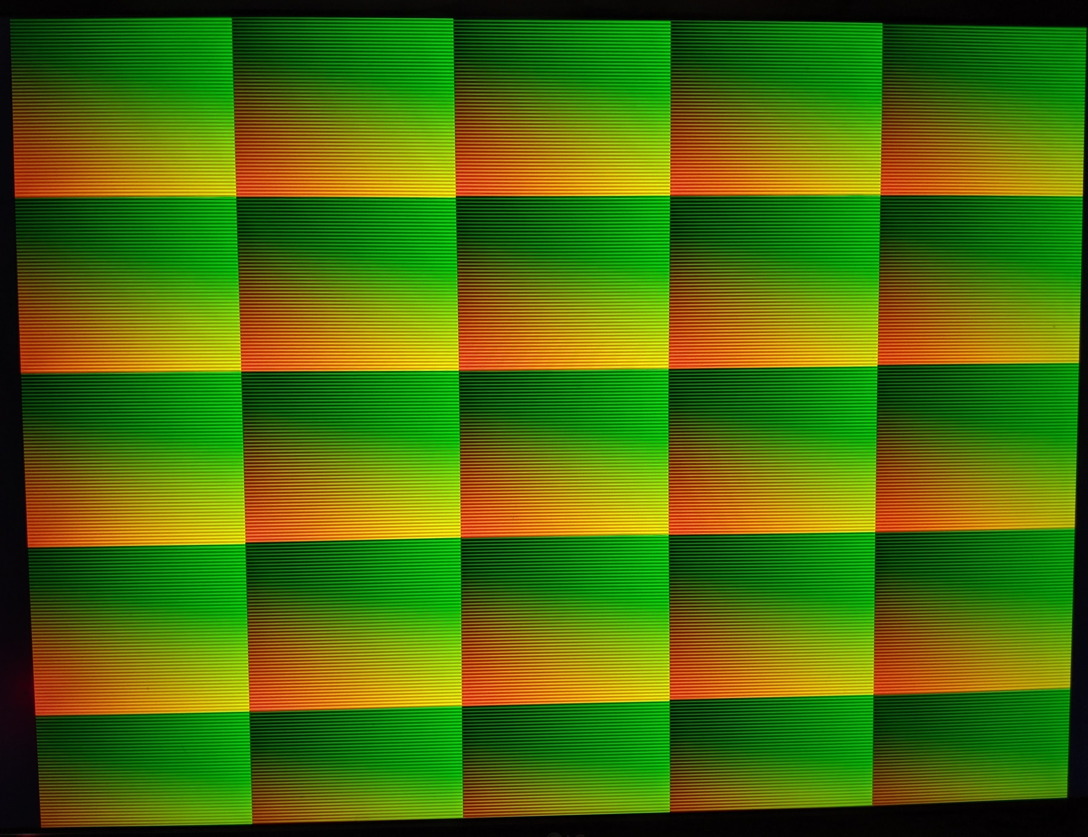
top/mkrvidor4000_quartus/mkrvidor4000_top.svfor a usage example with clock domain crossing. A dual-clock FIFO is used to move data from the SDRAM to HDMI to display a test pattern. The test pattern is composed only of red and green. If you see blue, the pattern is incorrect. - Read through the parameters in
sdram_controller.svand tailor any instantiations to your situation. - Please create an issue if you run into a problem or have any questions. Make sure you have consulted the troubleshooting section first.
- CAS latency: the time (in clocks) after the column-address is set for the command to return data
- Precharge: a required step in DRAM operation that sets the line voltage to Vcc / 2 (3.3V / 2) in anticipation of the next operation
- Refresh: restores the charge in the cells by rewriting them, preventing the loss of data
- Self Refresh: a low power mode where the SDRAM chip is able to refresh itself
- DQM: turning on DQ-masking disables the output during a read and masks the input during a write. Used to avoid I/O contention.
- Make sure you've set the IO standard for the pins connected to the DRAM chip as LVTTL 3.3V
- SystemVerilog users: make sure you are using
wireinstead oflogicfor DQ and the clock. This caused synthesis issues for me where the pins were stuck at GND or VCC when they were clearly being driven. - If you see noise or data corruption, check your FPGA driver strength, check if the SDRAM chip has configurable driver strength, and try lowering the clock
- Self Refresh Mode
- Optimizations
- Conditionally avoid manual precharging
- Manual precharging can assume spatial locality by only precharging if the next command is for a different column-address
- Bank activation: if the row address and bank are the same, can you do a repeated read/write? (yes until tmax bank active)
- Command pipelining: you could activate another bank while a write/read is being done (some overhaul of the state machine is needed here)
- Conditionally avoid manual precharging
These documents are not hosted here! They are available directly from Alliance Memory.
