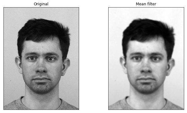
The task is to develop a mean filter algorithm using VHDL and Basys3 FPGA. The mean filter is capable of removing the noise from an image by blurring the image. A 3x3 kernel is used for this implementation. The kernel will be moving through the image. During the moving, the average value of the pixels of the image which are covered by the kernel will be calculated. Then the pixel value of the center pixel at that instance will be replaced with the calculated average value. This image transformation reduces the noise of the image and smooths the image.
The high level architecture of the system is as follows.

The main task of the scheduler is to manage the image convolution process. The process is initiated by the scheduler in the process when user input is given. Then the row and column values of the pixel that the mean value should be obtained are fed to the Mean Filter module and the init_single_op flag is raised. All the row and column values of the pixels are fed to the Mean Filter module pixel by pixel.

Mean filter module is used for the purpose of calculating the pixel value of a given pixel of the final image. Row and column values are given as 5 bit values with address of the memory location of the output BRAM component. Here a 3x3 kernel is used for the convolution.

Then respective 9 pixel values are retrieved from the input BRAM. For that first need to calculate the memory location of the pixel value as here the input image is considered as 1D array. For that below formula is used. col_offset and row_offset variables are used for the purpose of implementing a for loop. Both variables are initialized as -1 and it loops until row_offset gets value 1. Calculated address value is used to get the pixel value and added to a global variable sum. Final value for the output image is gained by dividing it by 9 which is the kernel size. Then it is sent to the output bram with the address of the output BRAM.
 col_offset and row_offset variables are used for the purpose of implementing a for loop. Both variables are initialized as -1 and it loops until row_offset gets value 1.
Calculated address value is used to get the pixel value and added to a global variable sum.
Final value for the output image is gained by dividing it by 9 which is the kernel size. Then it is sent to the output bram with the address of the output BRAM.
col_offset and row_offset variables are used for the purpose of implementing a for loop. Both variables are initialized as -1 and it loops until row_offset gets value 1.
Calculated address value is used to get the pixel value and added to a global variable sum.
Final value for the output image is gained by dividing it by 9 which is the kernel size. Then it is sent to the output bram with the address of the output BRAM.

Block Rams are used to store the input image and the calculated output image. BRams are created using the Block Memory Generator IP core. The BRams were configured using the following settings.
| Parameter | Value |
|---|---|
| Interface Type | Native |
| Memory Type | Simple Dual-Port RAM |
| Write Width | 8 |
| Write Depth | 324 |
The data of the input image is written to Block Ram 1 by the UART Handler module which is received by UART and the data is read by the Mean Filter module. Furthermore, the data of the calculated output image is written to the Block Ram 2 by Mean FIlter module and the data is read by the UART Handler module to transmit using UART.

The UART Communication between the Computer and FPGA is achieved by the UART Lite IP and it has four registers to conduct this UART communication as follows.
| Address Offset | Register Name | Description |
|---|---|---|
| 0h | Rx FIFO | Receive data FIFO |
| 04h | Tx FIFO | Transmit data FIFO |
| 08h | STAT_REG | UART Lite status register |
| 0Ch | CTRL_REG | UART Lite control register |
UART Communication is achieved by doing read operations and write operations to the above four registers. The read operations and write operations are done using AXI protocol which is a protocol used to communicate in network-on-chip systems.

UART handlers receive the input image from the Rx line and load the input image to the first BRAM. Then after finishing the whole process BRAM sends the resulting image to the Tx line.
