The J-Link OB (for On-Board) is essentially a microcontroller-based, single-chip, J-Link that goes right on the evaluation board. It is compatible with, and has the same features as, J-Link BASE with reduced, but still great, performance.
The microcontroller that is used as a J-Link OB (on the left side of the evaluation board in the diagram below) has a USB-interface on its left side (facing the host) and a JTAG/SWD + SWO interface on its right side (facing the target device).


J-Link OB can support JTAG or SWD interfaces for debugging and programming. For the QPG6xxx series controllers, the SWD interface is used. To enable this feature on the prototyping board, specific pins are needed to connect to the J-Link OB circuit. Here below is the list of necessary pins.
| Pin | Function | Description |
|---|---|---|
| 22 (GPIO5) | PROG_ENn |
Pin for forcing QPG6105 to go into programming mode. |
| 23 (GPIO6) | SWDIO |
Bidirectional data pin for programming and debugging. |
| 24 (GPIO7) | SWCLK |
Clock pin for programming and debugging. |
| 27 (GPIO8) | PROG_MOSIUART0_RX |
Optional pin for enabling SPI programming. By default, it is used as UART0_RX. |
| 28 (GPIO9) | SWOUART0_TX |
Optional pin for enabling data tracing during debug. By default, it is used as UART0_TX. |
| 26 (RESETn) | RESETn |
Pin for hard resetting the QPG6105. |
For more information on designing with J-Link OB on your own, please refer to Segger through the below link.
https://www.segger.com/products/debug-probes/j-link/models/j-link-ob/
Segger Tooling not working
ERROR: Could not connect to target.is shown in log when connecting with J-Link tools (i.e. J-Flash Lite, ...)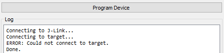

Unable to program by Drag-and-drop
Connect erroris shown in the FAIL.TXT after dropping an image to the JLINK drive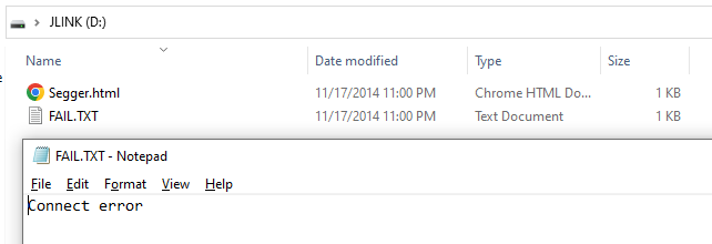

Large capacitance (> 200nF/0.2uF) is connected to the RESETn line. This causes the voltage on RESETn to rise slower than the J-Link tools expect once reset is released. When the timeout of J-Link tools expires, the voltage is still under the threshold and reset is still being held in to the QPG6105. So the QPG6105 is not responsive and cannot be connected by the J-Link or J-Link OB.
- Ensure the target is connected properly as the instructions found here.
- Check the capacitor placed on the RESETn line to ensure whether the capacitance is exceeding 200nF (0.2uF) or not.
In case of the IoT Dev Kit for QPG6105, the capacitor placed on the radio board is only 22nF, so no issue will be seen.
If so, please follow the below steps for a fix.
In case of Segger Tooling not working, the newer release (>= v7.68b) of the J-Link tools lengthened the delay after releasing the reset pin as part of the device specific connect sequence.
Further detail can be seen in the v7.68b Release Note from Segger.
J-Link v7.86b Release Note
Please upgrade the Segger J-Link Software pack to version >= v7.68b.
J-Link Bundle Download
In case of Drag-and-drop failure, the large capacitance on RESETn placed on the radio board or inside the module is not compatible with carrier board of production year-week < 2310.
The production year-week is shown on the carrier board as highlighted by a RED box in the below image.

Please request for a new Smart Home & Lighting Carrier Board from you Qorvo representative / distrbutor if your board is outdated.