Language selection

Search

Patent 2160751 Summary

Third-party information liability

Some of the information on this Web page has been provided by external sources. The Government of Canada is not responsible for the accuracy, reliability or currency of the information supplied by external sources. Users wishing to rely upon this information should consult directly with the source of the information. Content provided by external sources is not subject to official languages, privacy and accessibility requirements.

Claims and Abstract availability

Any discrepancies in the text and image of the Claims and Abstract are due to differing posting times. Text of the Claims and Abstract are posted:

  • At the time the application is open to public inspection;
  • At the time of issue of the patent (grant).
(12) Patent: (11) CA 2160751
(54) English Title: SHIELDED SWITCH
(54) French Title: CLAVIER BLINDE
Status: Expired and beyond the Period of Reversal
Bibliographic Data
(51) International Patent Classification (IPC):
  • H05K 9/00 (2006.01)
  • H03K 17/98 (2006.01)
  • H04B 15/02 (2006.01)
  • H04M 1/03 (2006.01)
  • H05K 1/02 (2006.01)
(72) Inventors :
  • KOMRSKA, DEAN MICHAEL (United States of America)
  • JOHNSON, DALE GORDON (United States of America)
(73) Owners :
  • MOTOROLA, INC.
(71) Applicants :
(74) Agent: GOWLING WLG (CANADA) LLP
(74) Associate agent:
(45) Issued: 1999-09-07
(22) Filed Date: 1995-10-17
(41) Open to Public Inspection: 1996-05-11
Examination requested: 1995-10-17
Availability of licence: N/A
Dedicated to the Public: N/A
(25) Language of filing: English

Patent Cooperation Treaty (PCT): No

(30) Application Priority Data:
Application No. Country/Territory Date
08/336,962 (United States of America) 1994-11-10

Abstracts

English Abstract


An EMI shielded keypad (10) or switch for a radiotelephone (50) has
a non-conductive cover (12) attached to a printed circuit board (PCB) (14).
The PCB (14) has a ground pad (20) and a plurality of metal traces (26) on a
first surface (16) that attaches to the cover (12). The cover (12) is made of a
flexible, preferably clear material, such as mylar and has a dimple (28)
centered over the ground pad (20). A bubble (30) is centered over the
plurality of conductive traces (26). A conductive coating (32) is selectively
applied to the mating surface (34) of the cover (12), so that the conductive
coating (32) in the bubble (30) is electrically isolated. By pressing on the
bubble (30) electrically contact is established between the plurality of traces
(26), thus the bubble and the traces (26) define a switch.


Claims

Note: Claims are shown in the official language in which they were submitted.

THE EMBODIMENT OF THE INVENTION IN WHICH AN EXCLUSIVE PROPERTY OR
PRIVILEGE IS CLAIMED ARE DEFINED AS FOLLOWS:
1. An EMI shielded keypad comprising:
a printed circuit board including a first surface and a plurality of metal
traces on
the first surface; and
a cover attached to the first surface of the printed circuit board, the cover
including, a flexible, non-conductive, essentially planar surface having an
attaching face;
a dome formed in the planar surface, convex relative the first surface, and
centered over the plurality of metal traces; and
a conductive coating selectively applied on the attaching face of the planar
surface such that a gap is provided in the conductive coating to provide
electrical
isolation of the portion of the conductive coating on the dome;
whereby pressing the dome towards the plurality of metal traces causes
electrical coupling between the plurality of metal traces via the portion of
the conductive
coating on the dome coming into contact with the plurality of metal traces.
2. The EMI shielded keypad of claim 1, wherein the printed circuit board
further
including a non-conductive coating selectively applied to the first surface
for electrically
isolating other metal traces on the first surface from the conductive coating.
3. The EMI shielded keypad of claim 2, wherein the non-conductive coating is
formed by a solder mask.
4. The EMI shielded keypad of claim 1, wherein an adhesive is used to attach
the
cover to the printed circuit board.
5. The EMI shielded keypad of claim 1, wherein the printed circuit board
further
including a ground pad on the first surface, wherein the conductive coating is
electrically
coupled with the ground pad except for the conductive coating under the dome.
6. The EMI shielded keypad of claim 5, wherein the cover further including a
dimple
formed in the planar surface and, convex relative the first surface to
electrically couple
the conductive coating with the ground pad except for the conductive coating
under the
dome.

7. An EMI shielded keypad comprising:
a printed circuit board, comprising:
a plurality of metal traces having an exposed portion on a first surface of
said printed circuit board; and
a ground pad on the first surface of the printed circuit board; and
a cover attached to the first surface of the printed circuit board said cover
comprising;
a flexible non-conductive essentially planar surface having an attaching
face;
a dome centered over the exposed portion of said plurality of metal
traces; and
a conductive coating on the attaching face of the planar surface, wherein
the conductive coating is silver, said conductive coating contacting the
ground pad;
whereby pressing the dome onto the plurality of metal traces causes electrical
conduction between the traces.
8. A radiotelephone having a receiver, a transmitter, an antenna connected to
the
receiver and the transmitter, and a processor controlling the radiotelephone,
said
radiotelephone comprising:
a rectangular housing;
a visual display on one surface of said housing controlled by said processor;
and
a EMI shielded keypad on said one surface of said housing controlled by said
processor, wherein said EMI Shielded keypad comprises, a printed circuit board
having
a plurality of exposed conductors, a flexible non-conductive cover attached to
the
printed circuit board said cover having a bubble over the plurality of exposed
conductors
and Said cover having a conductive coating on the surface adjacent the printed
circuit
board, wherein the conductive coating is selectively applied to the bubble and
the
bubble is electrically isolated from the rest of the conductive coating.
9. The radiotelephone of claim 8, wherein the conductive coating is an
adhesive
for holding the cover onto the printed circuit board.
10. The radiotelephone of claim 8, wherein the printed circuit board further
has a
ground pad that makes electrical contact with the conductive coating on the
cover.

11. A radiotelephone having a receiver, a transmitter, an antenna connected to
the
receiver and the transmitter, and a processor controlling the radiotelephone,
said
radiotelephone comprising:
a rectangular housing;
a visual display on one surface of said housing controlled by said processor;
and
a EMI shielded keypad on said one surface of said housing controlled by said
processor, wherein said EMI shielded keypad comprises, a printed circuit board
having
a plurality of exposed conductors, a flexible non-conductive cover attached to
the
printed circuit board, said cover having a bubble over the plurality of
exposed
conductors and said cover having a conductive coating on the surface adjacent
the
printed circuit board, wherein the conductive coating is silver.
12. The radiotelephone of claim 11, further including a non-conductive
adhesive for
holding the cover onto the printed circuit board.

Description

Note: Descriptions are shown in the official language in which they were submitted.


. 21647~~.
SHIELDED SWITCH
Field of the Invention
The present invention relates generally to the field of
radiotelephones and more generally to EMI shielding for radiotelephones.
Background of the Invention
l0
Electromagnetic interference (EMI) poses two concerns for
radiotelephones. The first concern is EMI entering ,the radiotelephone
circuitry and introducing noise, which can degrade signal reception and
cause improper operation of the radiotelephone. The second concern is
the amount of EMI emitted from the radiotelephone. All electronic
products have to meet FCC regulations on the amount of EMI they can
emit.
Generally, the approach to shielding from EMI is to provide a
conductive, usually metal, enclosure either around the sour;.e of the EMI
or around the electronic circuitry that is most susceptible to EMI. Often
the conductive enclosure is grounded. In radiotelephones this usually
means placing metal enclosures over EMI emitters and susceptible
circuitry. However, this is usually not sufficient so the plastic housing
holding the radiotelephone is coated with a metallic paint or covered with
a metallic screen.
While the metal enclosures and metallized housings provide
adequate EMI shielding, there is a constant drive to reduce the
manufacturing costs of radiotelephones. The process of shielding the
housings is relatively expensive. To avoid shielding the housing more
3o metal enclosures can be used to cover the electronic circuitry. While this
is less expensive than shielding the housing it provides an inadequate
level of EMI shielding for the radiotelephone. Thus there exists a need for
a less expensive way to provide EMI shielding in a radiotelephone.

-2-
Brief Description of the Drawings
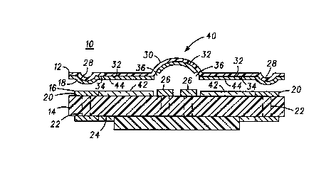
FIG. 1 is a cross section of a keypad circuit board;
FIG. 2 is a block diagram of a radiotelephone; and
FIG. 3 is a top left perspective view of a radiotelephone.
Description of the Preferred Embodiments
A solution to providing cheaper EMI shielding involves combining
the function of shielding with a keypad. FIG. 1 shows a cross section of a
keypad 10 with EMI shielding. The keypad 10 has a cover 12 and a printed
circuit board 14. The printed circuit board (PCB) 14 has a first surface 16
that abuts a mating surface 18 of the cover 12. The first surface 16 has a
ground pad 20 connected to a conductive feed through 22 which
electrically connects the ground pad 20 to PCB ground on the second
surface 24. A plurality of exposed metal traces 26 define a switch contact,
on the first surface of the PCB 14.
2o The cover 12 is made of a flexible material, such as mylar. The
cover 12 has a dimple 28 centered over the ground pad 20 to assure
electrical contact. A convex bubble or dome 30 in the cover 12 is centered
over the plurality of metal traces 26. A conductive coating 32, preferably
silver, is stenciled onto a mating surface 34 of the cover 12 which attaches
to the first surface 16 of the PCB 14.
The conductive coating 32 is applied selectively so that there is a gap
36 in the coating 32 to provide electrical isolation of the bubble 30. This
electrically isolated bubble makes up a second contact of a switch 40.
When pressure is applied to the bubble 30 the conductive coating 32 makes
3o electrical contact with the plurality of traces 26, thus closing the switch
40.
Upon release the bubble 30 rebounds to its non-contact position, (as shown
if FIG. 1) thus opening the switch 40. The bubble 30 is about the size of a

216 ~3 '~ ~ ~.
-3-
fingertip which is the intended object to provide pressure. B~placing a
number of these switches on the PCB 14 and cover 12 you can make a
keypad. Normally, the keypad 10 has a rubber template over the cover 12
and LEDs on the PCB 14. The template has the numerals written in a light
color and the light from the LEDs is dispersed by the translucent rubber
template to light up the .numerals. .
Often the PCB 14 has a solder mask (non-conductive coating) 42
which electrically isolates other conductive traces from the conductive
coating 32. The cover 12 can be attached to the PCB 14 by a number of
o methods including mechanical fasteners, pressure fit and an adhesive or
an adherent 44. The adhesive 44 can be applied to the conductive coating
32, except under the bubble 30 and dimple 28 or a conductive adhesive 44
could replace the conductive coating 32, except bubble 30. On the other
hand, a non-conductive adhesive 44 applied everywhere except under the
dimple 28 and bubble 30 could replace the solder mask 42.
The structure of FIG. 1 provides a grounded conductive plane across
the entire keypad 10 expect for the bubbles 30. This results is an effective,
low cost, EMI shield for the circuitry covered by the keypad 10.
The keypad 10 of FIG. 1 could be used with a wide variety of
2o electronic instruments, such as telephones, fax machines, calculators,
personal digital assistants, etc. The block diagram of FIG. 2 s:~ows a radio
telephone 50, in which the keypad 10 of FIG. 1 may be advantageously
used. The radiotelephone 50 has an antenna 52 connected to a duplexer
54. The duplexer 54 isolates the energy from a transmitter 56 and a
receiver 58. A processor 60 controls the transmitter 56, the receiver 58, a
display 62 and the keypad 10 of FIG.1. The EMI shielded keypad 10
provides EMI protection for the radiotelephone 50 circuitry designated by
the processor 60, the transmitter 56, the receiver 58 and the duplexer 54
blocks.
3o FIG. 3 shows a perspective view of a radiotelephone 50 with the EMI
shielded keypad 10. When the keypad 10 is used with metal enclosures
over the most sensitive circuitry, it provides a low cost effective EMI
solution for the radiotelephone 50. When compared to the conventional
solution of metallizing the housing 64 of the radiotelephone 50 and metal
enclosures over the sensitive circuitry, this solution provides a significant
reduction in the cost of shielding the radio.

2160751
-4-
__
A number of modifications could be made by those skilled in the art
without departing from the scope of the invention. For instance, the
dimple 28 may be eliminated by wrapping the cover 12 around circuit
board 14. The dome 30 may be flexible metal dome adhered to the mating
surface 18 of the cover 12. Finally, the cover 12 may be attached to the PCB
14 by a number of methods, such as soldering, spot welding, mechanical fit
and others.
1o What is claimed is:

Representative Drawing
A single figure which represents the drawing illustrating the invention.
Administrative Status

2024-08-01:As part of the Next Generation Patents (NGP) transition, the Canadian Patents Database (CPD) now contains a more detailed Event History, which replicates the Event Log of our new back-office solution.

Please note that "Inactive:" events refers to events no longer in use in our new back-office solution.

For a clearer understanding of the status of the application/patent presented on this page, the site Disclaimer , as well as the definitions for Patent , Event History , Maintenance Fee  and Payment History  should be consulted.

Event History

Description Date
Inactive: IPC expired 2009-01-01
Inactive: IPC from MCD 2006-03-12
Time Limit for Reversal Expired 2002-10-17
Letter Sent 2001-10-17
Grant by Issuance 1999-09-07
Inactive: Cover page published 1999-09-06
Inactive: Final fee received 1999-06-02
Pre-grant 1999-06-02
Letter Sent 1999-03-10
Notice of Allowance is Issued 1999-03-10
Inactive: IPC assigned 1999-02-25
Inactive: IPC removed 1999-02-25
Inactive: Approved for allowance (AFA) 1999-02-24
Amendment Received - Voluntary Amendment 1998-12-18
Inactive: S.30(2) Rules - Examiner requisition 1998-09-18
Inactive: Status info is complete as of Log entry date 1997-12-01
Inactive: Application prosecuted on TS as of Log entry date 1997-12-01
Application Published (Open to Public Inspection) 1996-05-11
Request for Examination Requirements Determined Compliant 1995-10-17
All Requirements for Examination Determined Compliant 1995-10-17

Abandonment History

There is no abandonment history.

Maintenance Fee

The last payment was received on 1998-09-22

Note : If the full payment has not been received on or before the date indicated, a further fee may be required which may be one of the following

  • the reinstatement fee;
  • the late payment fee; or
  • additional fee to reverse deemed expiry.

Please refer to the CIPO Patent Fees web page to see all current fee amounts.

Fee History

Fee Type Anniversary Year Due Date Paid Date
Request for examination - standard 1995-10-17
MF (application, 2nd anniv.) - standard 02 1997-10-17 1997-09-19
MF (application, 3rd anniv.) - standard 03 1998-10-19 1998-09-22
Final fee - standard 1999-06-02
MF (patent, 4th anniv.) - standard 1999-10-18 1999-09-17
MF (patent, 5th anniv.) - standard 2000-10-17 2000-09-20
Owners on Record

Note: Records showing the ownership history in alphabetical order.

Current Owners on Record
MOTOROLA, INC.
Past Owners on Record
DALE GORDON JOHNSON
DEAN MICHAEL KOMRSKA
Past Owners that do not appear in the "Owners on Record" listing will appear in other documentation within the application.
Documents

To view selected files, please enter reCAPTCHA code :


To view images, click a link in the Document Description column. To download the documents, select one or more checkboxes in the first column and then click the "Download Selected in PDF format (Zip Archive)" or the "Download Selected as Single PDF" button.

List of published and non-published patent-specific documents on the CPD .

If you have any difficulty accessing content, you can call the Client Service Centre at 1-866-997-1936 or send them an e-mail at CIPO Client Service Centre.


Document
Description 
Date
(yyyy-mm-dd) 
Number of pages   Size of Image (KB) 
Abstract 1996-03-08 1 22
Cover Page 1996-03-08 1 15
Description 1997-04-22 4 160
Description 1995-11-09 4 157
Claims 1996-03-08 2 62
Drawings 1996-03-08 1 25
Claims 1998-12-18 3 111
Cover Page 1999-08-31 1 38
Representative drawing 1999-08-31 1 10
Representative drawing 1998-05-11 1 12
Reminder of maintenance fee due 1997-06-17 1 109
Commissioner's Notice - Application Found Allowable 1999-03-10 1 164
Maintenance Fee Notice 2001-11-14 1 178
Correspondence 1999-06-02 1 28
Fees 1999-09-17 1 31